
Organic electroluminescence device and manufacturing method thereof

An electroluminescent device, organic technology, applied in the direction of electric solid device, semiconductor/solid state device manufacturing, electrical components, etc., can solve the problems of large light loss and low light extraction efficiency

Inactive Publication Date: 2015-03-18
OCEANS KING LIGHTING SCI&TECH CO LTD +2
View PDF0 Cites 2 Cited by
  • Summary
  • Abstract
  • Description
  • Claims
  • Application Information

AI Technical Summary

Problems solved by technology

[0004] Based on the above problems, the present invention provides an organic electroluminescent device, which solves the problems of large light loss and low light extraction efficiency of the organic electroluminescent device. The organic electroluminescent device of the present invention has improved luminous efficiency and enhanced light extraction efficiency

Method used


Image

  • Organic electroluminescence device and manufacturing method thereof
  • Organic electroluminescence device and manufacturing method thereof

Examples


Embodiment 1

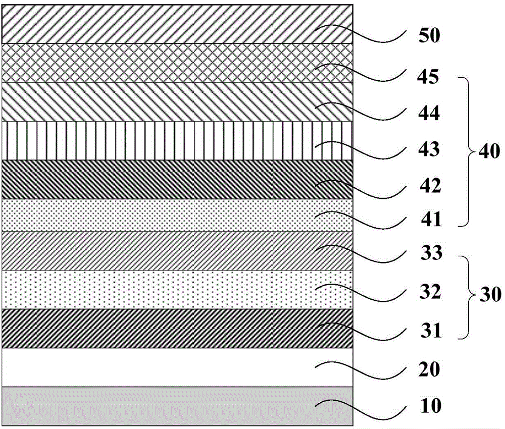
[0047] figure 1 A schematic structural diagram of an organic electroluminescent device provided in this embodiment. like figure 1 As shown, the organic electroluminescent device is sequentially stacked with a substrate 10 , an anode 20 , a scattering layer 30 , an organic light-emitting functional layer 40 and a cathode 50 from bottom to top. Wherein, the scattering layer 30 includes a first doped layer 31, an iron salt layer 32, and a second doped layer 33 that are stacked sequentially from bottom to top; The hole injection layer 41 , the hole transport layer 42 , the light emitting layer 43 , the electron transport layer 44 and the electron injection layer 45 . More specifically, the grade of the substrate 10 is N-LASF44, the anode 20 is a 150nm thick ITO layer, and the first doped layer 31 is a 30nm thick F4-TCNQ:FeCl 3 layer, the iron salt layer 32 is 15nm thick FeCl 3 layer, the second doped layer 33 is 150nm thick 1T-NATA:TiO 2 layer, the hole injection layer 41 is ...

Embodiment 2

[0056] Embodiment 2: the preparation of a kind of organic electroluminescence device; Device structure is: glass substrate / IZO / 1T-NATA:FeBr 3 / Fe 2 S 3 / F4-TCNQ:TiO 2 / MoO 3 / NPB / ADN / TPBi / CsN 3 / Al.

[0057] Its preparation method is as follows:

[0058] (1) Use N-LAF36 optical glass as the substrate, rinse the glass substrate with distilled water and ethanol, and soak it in isopropanol for 12 hours.

[0059](2) Prepare an 80nm thick IZO anode film on the cleaned glass substrate by magnetron sputtering; control the acceleration voltage of magnetron sputtering to 300V, the magnetic induction intensity is about 50G, and the power density is 40W / cm 2 , the background vacuum is 2×10 -3 Pa.

[0060] (3) Prepare a scattering layer on the IZO anode film, including a first doped layer, an iron salt layer and a second doped layer that are sequentially stacked. First prepare the first doped layer, which is 1T-NATA:FeBr 3 , 1T-NATA with FeBr 3 The mass ratio is 40:1, using the...

Embodiment 3

[0064] Embodiment 3: the preparation of a kind of organic electroluminescence device; Device structure is: glass substrate / AZO / 2T-NATA:Fe 2 S 3 / FeBr 3 / 2T-NATA:TiO 2 / V 2 o 5 / TCTA / Alq3 / Bphen / LiF / Au. Its preparation method is as follows:

[0065] (1) The optical glass with brand name N-LASF31A is used as the substrate. After rinsing the glass substrate with distilled water and ethanol, soak it in isopropanol for 24 hours.

[0066] (2) Prepare a 300nm-thick AZO anode film on the cleaned glass substrate by magnetron sputtering; control the acceleration voltage of magnetron sputtering: 800V, magnetic induction: 200G, power density: 1W / cm 2 ,, the background vacuum is 5×10 -5 Pa.

[0067] (3) Prepare a scattering layer on the AZO anode film, including a first doped layer, an iron salt layer and a second doped layer that are sequentially stacked. Prepare the first doped layer first, the material is 2T-NATA:Fe 2 S 3 , 2T-NATA and Fe 2 S 3 The mass ratio is 10:1, therma...


PUM

PropertyMeasurementUnit
Thicknessaaaaaaaaaa
Thicknessaaaaaaaaaa
Thicknessaaaaaaaaaa

Abstract

The invention provides an organic electroluminescence device. The organic electroluminescence device comprises a glass substrate, and an anode, a scattering layer, an organic light-emitting functional layer and a cathode which are sequentially arranged on the glass substrate in a stacked manner; the scattering layer comprises a first doped layer, a ferric salt layer and a second doped layer which are sequentially arranged on the anode in a stacked manner; the first doped layer is made of a mixed material of an organic material and ferric salt, and the second doped layer is made of a mixed material of the organic material and titanium dioxide; the organic material is one of 2, 3, 5, 6-tetrafluoro-7, 7, 8, 8, -tetracyano-benzoquinodimethane, 4, 4, 4-tri(naphthyl-1-phenyl-ammonio) triphenylamine and dinaphthyl-N, N'-diphenyl-4, 4'-benzidine. The scattering layer is additionally arranged in the structure of the organic electroluminescence device, so that the light-emitting efficiency and the luminous efficiency of the device can be improved. The invention also provides a manufacturing device of the organic electroluminescence device.

Description

technical field [0001] The invention belongs to the field of organic electroluminescence, and in particular relates to an organic electroluminescence device and a preparation method thereof. Background technique [0002] Organic electroluminescent devices (OLEDs) have a series of advantages such as low driving voltage, high luminous brightness, wide luminous viewing angle, ultra-thin and light weight, and easy mass production. The requirement of capacity, its broad application prospect and the rapid advancement of technology in recent years make OLED become a research hotspot in the field of flat panel information display. [0003] In 1987, C.W.Tang and Van Slyke of Eastman Kodak Company in the United States reported a breakthrough in the research of organic electroluminescence. A high-brightness, high-efficiency double-layer organic electroluminescent device (OLED) has been prepared using ultra-thin film technology. Brightness up to 1000cd / m at 10V 2 , its luminous effic...

Claims


Application Information

Patent Timeline
IPC IPC(8): H01L51/50H01L51/52H01L51/54H01L51/56
CPCH10K50/854H10K71/00
Inventor 周明杰黄辉陈吉星王平
Owner OCEANS KING LIGHTING SCI&TECH CO LTD
Learn More