Wavy MoS2 nanosheet inlaid TiO2 dandelion nanosphere composite heterojunction semiconductor material and preparation method thereof

A composite heterojunction and dandelion technology, applied in chemical instruments and methods, physical/chemical process catalysts, chemical/physical processes, etc., can solve problems such as inapplicability to large-scale industrial production, complex synthesis process, and high production cost. Achieve low cost, enhanced catalytic performance, and high reproducibility

Inactive Publication Date: 2015-03-25
EAST CHINA NORMAL UNIV
View PDF1 Cites 13 Cited by
  • Summary
  • Abstract
  • Description
  • Claims
  • Application Information

AI Technical Summary

Problems solved by technology

[0003] Recently, the academic community has begun to try the combination of two semiconductor materials, and has achieved remarkable results in photocatalysis and lithium-ion batteries. However, most of the current preparation methods have harsh reaction conditions, complex synthesis processes, and high production costs, which are not suitable for large-scale applications. industrial production

Method used


Image

  • Wavy MoS2 nanosheet inlaid TiO2 dandelion nanosphere composite heterojunction semiconductor material and preparation method thereof
  • Wavy MoS2 nanosheet inlaid TiO2 dandelion nanosphere composite heterojunction semiconductor material and preparation method thereof
  • Wavy MoS2 nanosheet inlaid TiO2 dandelion nanosphere composite heterojunction semiconductor material and preparation method thereof

Examples


Embodiment 1

[0034] Example 1 Preparation of wavy MoS 2 Nanosheet mosaic dandelion TiO 2 Nanosphere Composite Heterojunction Semiconductor Materials

[0035] The specific steps of preparation are as follows:

[0036] (1) Add 2 mL of 35% hydrochloric acid and 4 mL of tetrabutyl titanate into a small Erlenmeyer flask and shake and mix. It is found that the reaction generates high temperature. At this time, the Erlenmeyer flask is placed in cold water to cool rapidly. After cooling completely, Slowly drop the mixed solution into a beaker containing 20mL oleic acid while stirring.

[0037] (2) After stirring for more than 15 minutes, it will be found that the color of the solution gradually changes from egg yellow to orange and remains unchanged. At this time, the mixed solution is added to a 50mL reaction kettle, sealed, and then heated in a vacuum oven at 180°C for 4 Hours, the reaction was completed and cooled to room temperature.

[0038] (3) Wash the white precipitate at the bottom of...

Embodiment 2

[0045] Example 2 Wave MoS of the present invention 2 Nanosheet mosaic dandelion TiO 2 Photocatalytic Performance Test of Nanosphere Composite Heterojunction Semiconductor Materials

[0046] The wavy MoS of the present invention prepared in the above-mentioned Example 1 2 Nanosheet mosaic dandelion TiO 2 Nanosphere composite heterojunction semiconductor materials, due to their large specific surface area and the formation of p-n junctions at the junction, make them comparable to pure TiO 2 The photocatalytic performance of dandelion nanospheres has been significantly improved. Wave MoS of the present invention 2 Nanosheet mosaic dandelion TiO 2 Nanosphere Composite Heterojunction Semiconductor Materials and TiO 2 Photocatalytic performance test of dandelion nanospheres, including specific steps:

[0047] (1) Take two identical brown jars, put 100ml of methylene blue solution in each bottle, the solution concentration is 10mg L -1 .

[0048] (2) Take the wave MoS of the...


PUM

PropertyMeasurementUnit
diameteraaaaaaaaaa

Abstract

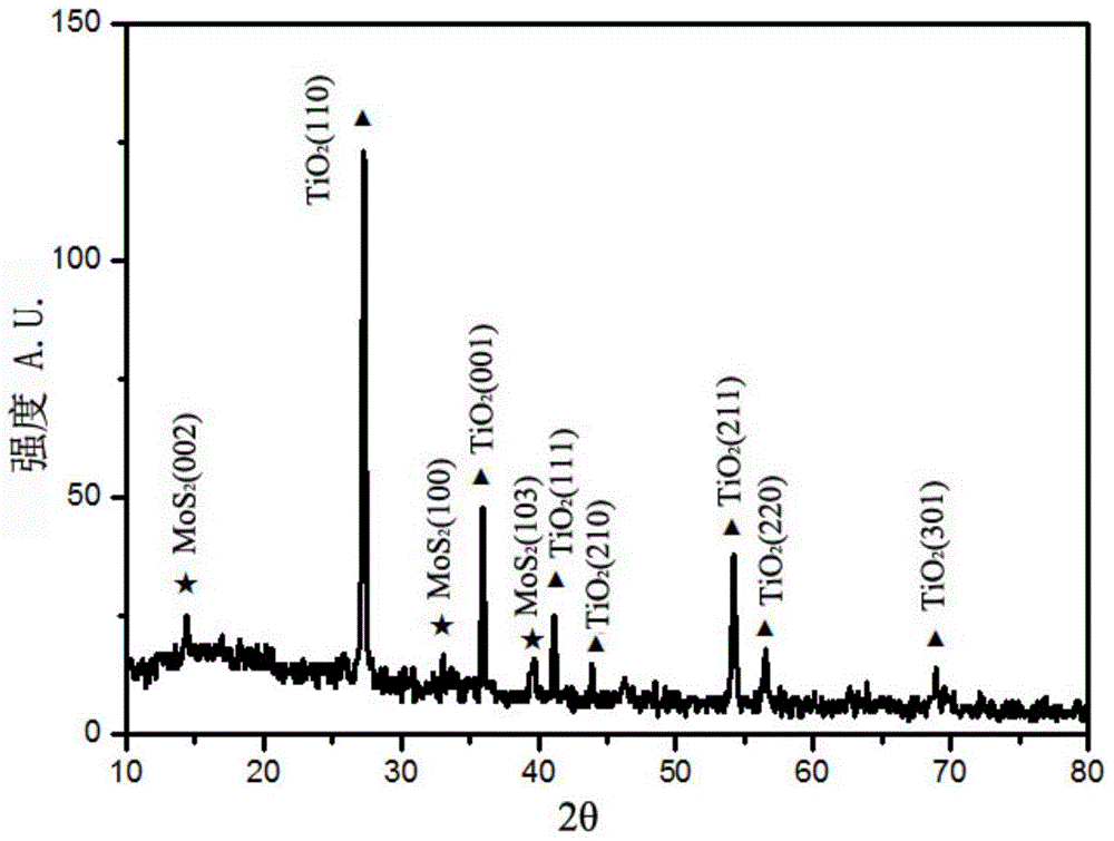
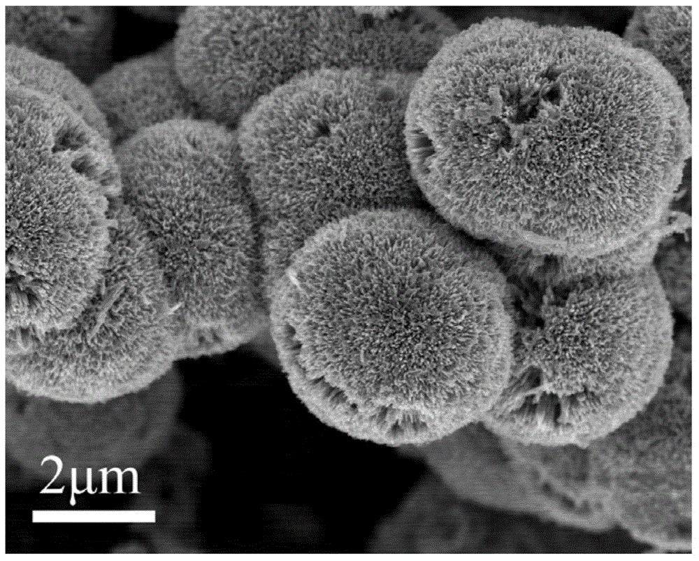
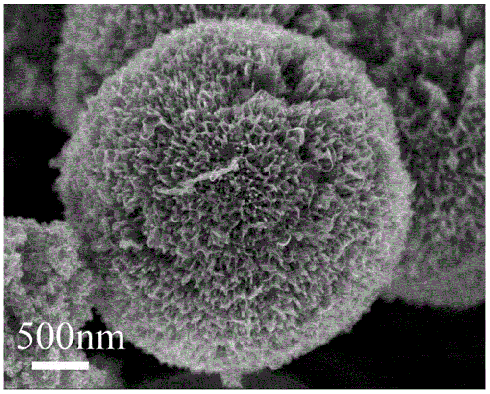
The invention discloses a wavy MoS2 nanosheet inlaid TiO2 dandelion nanosphere composite heterojunction semiconductor material. The wavy MoS2 nanosheet inlaid TiO2 dandelion nanosphere composite heterojunction semiconductor material contains MoS2 nanosheets and TiO2 dandelion nanospheres, wherein the MoS2 nanosheets penetrate through the space among nanorods on the TiO2 dandelion nanospheres uniformly and can be stably combined with gaps among the nanorods,. The invention also discloses a method for preparing the wavy MoS2 nanosheet inlaid TiO2 dandelion nanosphere composite heterojunction semiconductor material by a two-step solvent method. The wavy MoS2 nanosheet inlaid TiO2 dandelion nanosphere composite heterojunction semiconductor material and the method have the advantages that the preparation operation is simple, the yield is high and the cost is low, and the wavy MoS2 nanosheet inlaid TiO2 dandelion nanosphere composite heterojunction semiconductor material has great potential and wide application prospect in the fields of photo-catalytic industrial wastewater and field emission.

Description

technical field [0001] The invention belongs to the technical field of optoelectronic materials, semiconductor materials and devices, and in particular relates to a wave MoS 2 Nanosheet mosaic dandelion TiO 2 Nanosphere composite heterojunction semiconductor material and its preparation method. Background technique [0002] MoS 2 It is a metal sulfide with a narrow band gap, and it is also a typical two-dimensional layered semiconductor material. The layers are combined by weak van der Waals forces, making MoS 2 It has a wide range of applications in lithium-ion batteries, photocatalysis, field emission and sensors. Rutile TiO 2 It is a metal oxide with a wide bandgap, a three-dimensional semiconductor material that is easy to prepare and easy to undergo structural modification, TiO 2 Due to its special spherical structure and large (001) active surface, dandelion nanospheres are most commonly used in photocatalysis. [0003] Recently, the academic community has begun ...

Claims


Application Information

Patent Timeline
Patent Type & Authority Applications(China)
IPC IPC(8): B01J27/051B01J35/02
Inventor 傅豪郁可朱自强
Owner EAST CHINA NORMAL UNIV
Why Eureka
Try Eureka