Connection structure and anisotropic conductive adhesive

A connection structure, anisotropic technology, applied in the direction of conductive adhesives, connections, adhesives, etc., can solve problems such as difficult to repair and damaged appearance, and achieve the effect of preventing appearance damage and reducing light leakage

Active Publication Date: 2020-09-08
DEXERIALS CORP
View PDF9 Cites 0 Cited by
  • Summary
  • Abstract
  • Description
  • Claims
  • Application Information

AI Technical Summary

Problems solved by technology

[0003] However, when a defect such as a pinhole occurs in the decorative printed part, light leakage or the like occurs due to illumination of the backlight, and the appearance is impaired.
In addition, even if a pinhole is found in the decorative printing part by inspection, it is difficult to repair because the wiring has already been formed on the decorative layer

Method used


Image

  • Connection structure and anisotropic conductive adhesive
  • Connection structure and anisotropic conductive adhesive
  • Connection structure and anisotropic conductive adhesive

Examples


Embodiment 1

[0067] 60 parts by mass of polyester polyurethane resin (trade name: UR8200, produced by Toyobo Co., Ltd., dissolved in a mixed solvent of methyl ethyl ketone / toluene=50 / 50 to obtain 20 mass % of the result) as a film-forming resin, 34 parts by mass of free Base polymeric resin (trade name: EB-600, manufactured by Daicel Cytec Co., Ltd. (Daycel Cytec Co., Ltd.)), 1 part by mass of silane coupling agent (trade name: KBM-503, manufactured by Shin-Etsu Chemical Co., Ltd.), 1 mass part of phosphoric acid acrylate (trade name: P-1M, manufactured by Kyoei Chemical Co., Ltd.) and 4 mass parts of reaction initiator (trade name: Perhexa C (パーヘキサ C), manufactured by NOF Corporation) were blended In the adhesive, disperse conductive particles (trade name: AUL705, manufactured by Sekisui Chemical Co., Ltd.) so that the particle density is 5000 particles / mm 2 , and further dispersed 12 parts by mass of a titanium-based black pigment with an average primary particle diameter of 60 nm (trade...

Embodiment 2

[0070] The average primary particle diameter of 12 parts by mass is dispersed as a titanium-based black pigment (trade name: 13M-C, manufactured by Mitsubishi Materials) of 100 nm, and an anisotropic conductive film is prepared in the same manner as in Example 1 except that .

[0071] The transmittance of the anisotropic conductive film of Example 2 was 13.3%. In addition, the initial on-resistance of the bonded structure prepared using the anisotropic conductive film was 2.0Ω, and the on-resistance after the high-temperature and high-humidity test was 5.5Ω. In addition, the initial peel strength was 6.1 N / cm, and the peel strength after the high temperature and high humidity test was 4.0 N / cm. In addition, the evaluation of the light-shielding property was ⊚. Therefore, the overall decision is B. These results are shown in Table 1.

Embodiment 3

[0073] An anisotropic conductive film was prepared in the same manner as in Example 1 except that 12 parts by mass of a titanium-based black pigment (trade name: Tilack D, manufactured by Ako Kasei Co., Ltd.) having an average primary particle diameter of 800 nm was dispersed.

[0074] The transmittance of the anisotropic conductive film of Example 3 was 13.8%. In addition, the initial on-resistance of the bonded structure prepared using the anisotropic conductive film was 1.8Ω, and the on-resistance after the high-temperature and high-humidity test was 3.2Ω. In addition, the initial peel strength was 6.0 N / cm, and the peel strength after the high temperature and high humidity test was 4.3 N / cm.

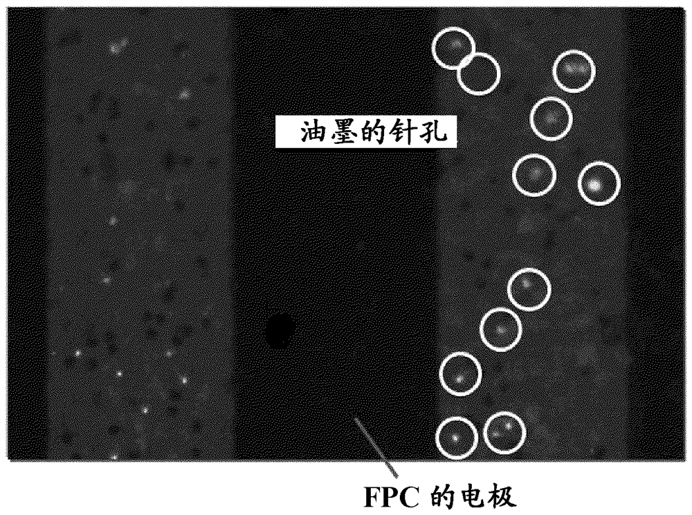
[0075] in addition, image 3 It is a photograph of the bonded structure produced using the anisotropic conductive film of Example 3, irradiated with light from the glass substrate for evaluation side in which pinholes were formed in advance, and observed with a metal microscope from...


PUM

PropertyMeasurementUnit
thicknessaaaaaaaaaa
electrical resistanceaaaaaaaaaa

Abstract

Provided are a bonded structure and an anisotropic conductive adhesive capable of preventing damage to the appearance of a decorative printed portion even when defects such as pinholes occur in the decorative printed portion. The bonded structure includes: a first electronic component 10 in which an electrode 13 is formed on a decorative layer 12; a second electronic component 20 in which an electrode 22 opposite to the electrode 13 of the first electronic component 10 is formed; The anisotropic conductive film 30 connecting the electrode 13 of the component 10 to the electrode 22 of the second electronic component 20; the anisotropic conductive film 30 is made of a cured product of an anisotropic conductive adhesive containing conductive particles 31 and black pigment form. Thereby, the light leakage of the pinhole of the decorative printing part can be reduced, and the design property of the decorative printing part can be maintained.

Description

technical field [0001] The present invention relates to a bonded structure and an anisotropic conductive adhesive in which electronic components are connected using an anisotropic conductive adhesive. Background technique [0002] In recent years, in order to increase the degree of design freedom, for example, in a cover glass integrated touch panel, it has been proposed to form electrodes on a decorative layer printed in a frame-like decoration on the outer periphery, and to bond the circuit member to the decorative layer. . [0003] However, when a defect such as a pinhole occurs in the decorative printed portion, light leakage or the like occurs due to irradiation of a backlight, thereby deteriorating the appearance. In addition, even if a pinhole is found in the decorative printed part by inspection, it is difficult to repair because the wiring has already been formed on the decorative layer. [0004] prior art literature [0005] patent documents [0006] Patent Doc...

Claims


Application Information

Patent Timeline
Patent Type & Authority Patents(China)
IPC IPC(8): G06F3/041C09J175/06C09J9/02C09J11/06
CPCG06F3/0412C09J9/02C09J175/06H01R11/01H05K1/14H01B1/22C09J11/04
Inventor 林慎一田中雄介
Owner DEXERIALS CORP
Why Eureka
Try Eureka