Array substrate doping method and doping equipment

An array substrate and substrate technology, applied in the field of substrate manufacturing, can solve the problems of complex doping process, process error, increased cost and production cycle, etc., and achieve the effect of simplifying process and reducing cost

Inactive Publication Date: 2015-04-01
TCL CHINA STAR OPTOELECTRONICS TECH CO LTD
View PDF6 Cites 13 Cited by
  • Summary
  • Abstract
  • Description
  • Claims
  • Application Information

AI Technical Summary

Problems solved by technology

[0005] According to the above description, it can be seen that the doping process in the prior art is relatively complicated, and three times of doping are required, which increases the cost and production cycle, and also easily leads to the problem of process error

Method used


Image

  • Array substrate doping method and doping equipment
  • Array substrate doping method and doping equipment
  • Array substrate doping method and doping equipment

Examples


Embodiment Construction

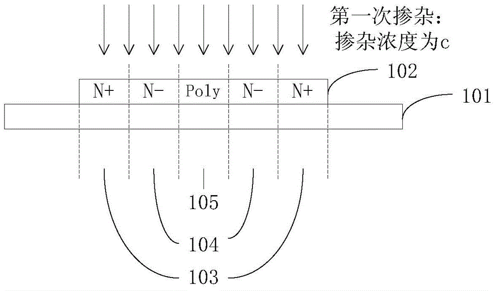
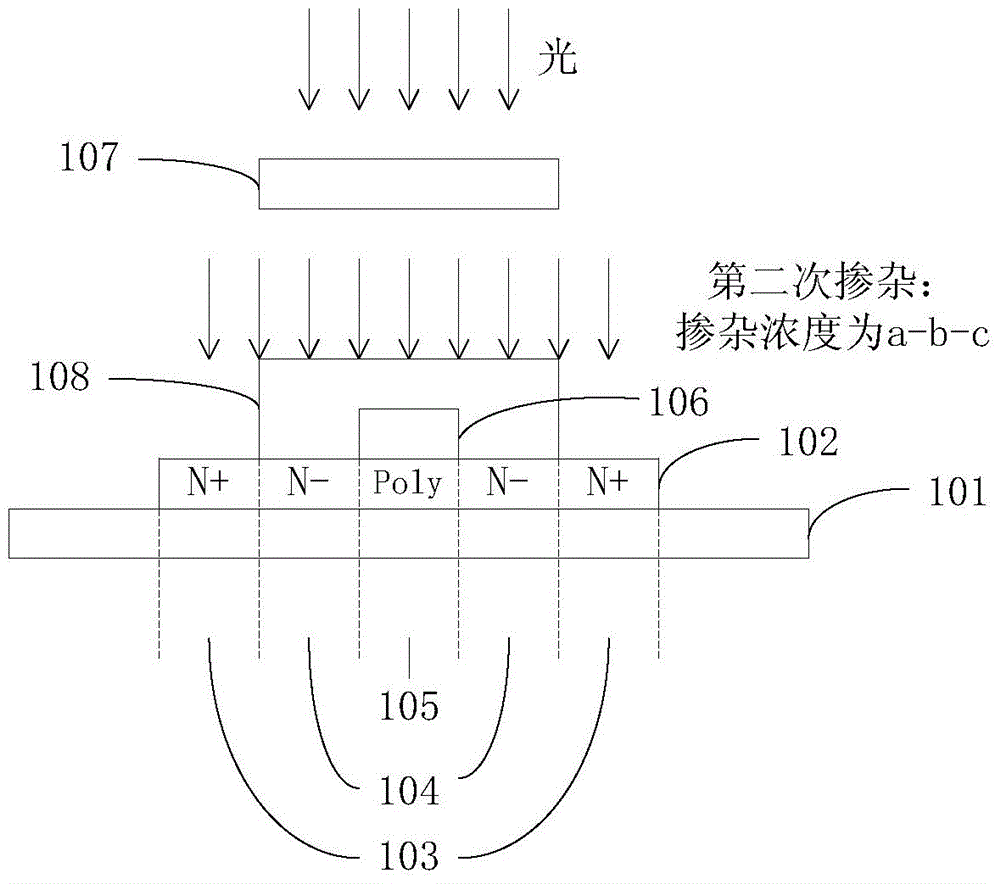
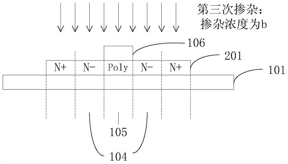
[0029] see figure 2 and image 3 , figure 2 is a schematic flow chart of the first embodiment of the doping method of the array substrate of the present invention, image 3 yes figure 2 The process schematic diagram corresponding to the first embodiment of the doping method shown, this embodiment provides a doping method, including steps:

[0030] S201: Provide a substrate, on which a region to be heavily doped, a region to be lightly doped, and a channel region to be doped are defined.

[0031] Generally speaking, processing holes, electroplating, etching, and arranging electronic components on the substrate 301 can realize electrical, magnetic, or optical functions. Doping a small amount of other elements or compounds in the substrate 301 can make the substrate 301 produce specific properties. Specifically, for example, doping phosphorus P or gallium Ga in a semiconductor silicon substrate can obtain n-type or p-type semiconductor materials respectively; in the inorg...


PUM


Abstract

The invention discloses an array substrate doping method and doping equipment. The method includes the following steps: providing an array substrate on which a region to be heavily doped, a region to be lightly doped and a channel region to be doped are defined; forming a photoresist layer on the array substrate through a photolithography process, wherein a first photoresist part is formed on the photoresist layer corresponding to the region to be heavily doped, a second photoresist part is formed on the photoresist layer corresponding to the region to be lightly doped, a third photoresist part is formed on the photoresist layer corresponding to the channel region to be doped, the first photoresist part is thinner than the second photoresist part, and the second photoresist part is thinner than the third photoresist part; carrying out a one-time doping in the region to be heavily doped, the region to be lightly doped and the channel region to be doped via the photoresist layer, so as to form a heavily doped region, a lightly doped region and a doped channel region at a time respectively corresponding to the region to be heavily doped, the region to be lightly doped and the channel region to be doped. With the steps, one-time doping is realized in the region to be heavily doped, the region to be lightly doped and the channel region to be doped on the array substrate; the process is simplified; the cost is reduced.

Description

technical field [0001] The present invention relates to the technical field of substrate manufacturing, in particular to a doping method and a doping device for an array substrate. Background technique [0002] Thin-film transistor (TFT) is the basic circuit component that controls the brightness of each pixel in a liquid crystal display. It is generally made of amorphous silicon structure. With the advancement of technology, more and more low-temperature polysilicon structures are used. This structure greatly The electrical performance of the thin film transistor is improved. [0003] Low-temperature polysilicon (LTPS) technology is used to form thin-film transistors. Generally, standard low-temperature polysilicon thin-film transistors have N-type heavily doped regions as source and drain electrodes on the polysilicon layer. Because the doping concentration of the two N-type heavily doped regions is relatively high High, and the distance between the conductor and the gate...

Claims


Application Information

Patent Timeline
Patent Type & Authority Applications(China)
IPC IPC(8): H01L21/22
CPCH01L21/22H01L21/67011H01L21/77H01L27/1214H01L2021/775G03F1/50H01L21/266H01L21/2652H01L21/223H01L29/66757H01L29/78678H01L29/78621H01L29/66765G03F7/2002H01L29/78675H01L27/127H01L27/1288H01L29/6675H01L29/66492G03F7/20G03F7/32
Inventor 薛景峰陈归郝思坤张鑫
Owner TCL CHINA STAR OPTOELECTRONICS TECH CO LTD
Why Eureka
Try Eureka