SOI (Silicon on Insulator) substrate folding grid insulating tunneling enhanced transistor and manufacturing method thereof

A gate insulation and transistor technology, applied in the field of ultra-large-scale integrated circuit manufacturing, can solve the problems of small forward conduction current, increase the difficulty of the process, and cannot substantially improve the tunneling probability of silicon materials, and achieve the effect of improving the production rate.

Inactive Publication Date: 2015-04-01
SHENYANG POLYTECHNIC UNIV
View PDF5 Cites 4 Cited by
  • Summary
  • Abstract
  • Description
  • Claims
  • Application Information

AI Technical Summary

Problems solved by technology

Although the degradation of this device performance can be alleviated by improving the structure of the gate electrode, when the device size is further reduced, the switching characteristics of the device will continue to deteriorate
[0003] Compared with MOSFETs, tunneling field-effect transistors (TFETs) proposed in recent years have improved their average subthreshold swing, but their forward conduction current is too small. Materials with a narrower band gap to generate the tunneling part of TFETs can increase the tunneling probability to improve switching characteristics, but increase the difficulty of the process
Using a high dielectric constant insulating material as the insulating dielectric layer between the gate and the substrate can improve the control ability of the gate to the electric field distribution of the channel, but it cannot essentially increase the tunneling probability of silicon materials. Therefore, for TFETs The forward conduction characteristic of the improvement is very limited

Method used


Image

  • SOI (Silicon on Insulator) substrate folding grid insulating tunneling enhanced transistor and manufacturing method thereof
  • SOI (Silicon on Insulator) substrate folding grid insulating tunneling enhanced transistor and manufacturing method thereof
  • SOI (Silicon on Insulator) substrate folding grid insulating tunneling enhanced transistor and manufacturing method thereof

Examples


Embodiment Construction

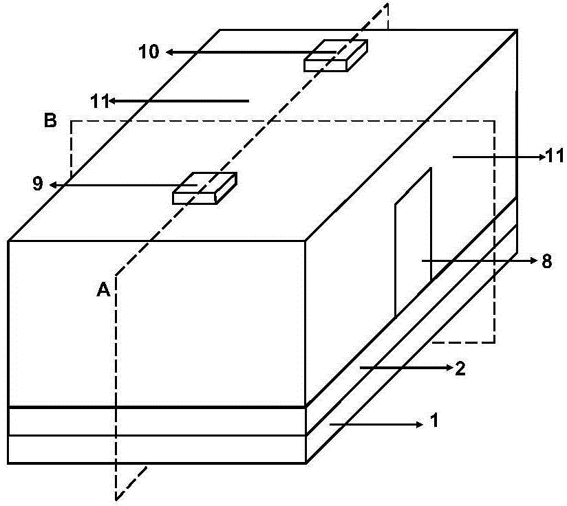
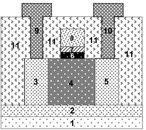
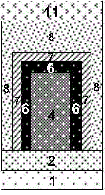
[0079] Below in conjunction with accompanying drawing, the present invention will be further described: figure 1 It is a schematic diagram of the three-dimensional structure of the SOI substrate folded gate insulation tunneling enhancement transistor formed on the SOI substrate of the present invention; figure 2 SOI substrate folded gate insulation tunneling enhanced transistor edge of the present invention figure 1 The two-dimensional cross-sectional view obtained after cutting on the middle A plane; image 3 SOI substrate folded gate insulation tunneling enhanced transistor edge of the present invention figure 1 The two-dimensional cross-sectional view obtained after cutting in the middle B plane; Figure 4 A schematic diagram of a three-dimensional structure after peeling off the blocking insulating layer 11 for the SOI substrate folded gate insulation tunneling enhancement transistor of the present invention; Figure 5 A schematic diagram of a three-dimensional structu...


PUM


Abstract

The invention relates to an SOI (Silicon on Insulator) substrate folding grid insulating tunneling enhanced transistor. The transistor is provided with insulating tunneling structures on the two sides and the upper surface of a base region simultaneously, so the insulating tunneling effect occurs on the two sides and the upper surface of the base region simultaneously under the control effect of a grid electrode, and thus the generation rate of tunneling current is improved; compared with MOSFETs (Metal Oxide Semiconductor Field Effect Transistor) or TFETs (Tunneling Field-Effect Transistor) devices of the same size, superior switching characteristic is realized by using the extremely sensitive mutual relation between the impedance of a tunneling insulating layer and the field intensity in the tunneling insulating layer; superior forward turn-on characteristic is realized by enhancing a tunneling signal through an emitter electrode; besides, the invention also provides specific manufacturing methods of an SOI substrate folding grid insulating tunneling enhanced transistor unit and an array of the enhanced transistor unit. According to the transistor, the working characteristic of a nanoscale integrated circuit unit is obviously improved; the transistor is suitable for popularization and application.

Description

Technical field: [0001] The invention relates to the field of ultra-large-scale integrated circuit manufacturing, and relates to a structure and a manufacturing method of an SOI substrate folded gate insulation tunneling enhanced transistor suitable for manufacturing high-performance ultra-high integrated integrated circuits. Background technique: [0002] The continuous shortening of the channel length of metal-oxide-semiconductor field-effect transistors (MOSFETs), the basic unit of integrated circuits, has led to a significant decline in the switching characteristics of the devices. The specific performance is that the subthreshold swing increases with the decrease of the channel length, and the static power consumption increases significantly. Although the degradation of the performance of the device can be alleviated by improving the structure of the gate electrode, when the size of the device is further reduced, the switching characteristics of the device will continue...

Claims


Application Information

Patent Timeline
Patent Type & Authority Applications(China)
IPC IPC(8): H01L29/739H01L29/423H01L21/331
CPCH01L29/423H01L29/66325H01L29/739
Inventor 靳晓诗吴美乐刘溪揣荣岩
Owner SHENYANG POLYTECHNIC UNIV
Why Eureka
Try Eureka