Three-dimensional integrated wafer-level package structure and package method for high-frequency IPD (Integrated Passive Device) module

A technology of wafer-level packaging and three-dimensional integration, which is applied in the direction of additional/integrated components of printed circuit boards, printed circuits assembled with electrical components, printed circuits connected with non-printed electrical components, etc., which can solve the problem of crowded PCB wiring areas, increased Problems such as large signal distributed capacitance and increased wiring amount, etc., achieve the effect of miniaturization of devices and systems, reduction of interference, and reduction of area

Active Publication Date: 2015-04-01
NAT CENT FOR ADVANCED PACKAGING
View PDF6 Cites 10 Cited by
  • Summary
  • Abstract
  • Description
  • Claims
  • Application Information

AI Technical Summary

Problems solved by technology

[0003] However, the radiation generated by traditional RF IPD devices is more likely to be coupled to the signal path of the PCB system board, generating radio frequency noise, which interferes with the circuit on the PCB system board, and affects the audio and video call quality of the mobile phone.
[0004] An effective way to solve the problem of signal interference between the RF IPD chip and the PCB system board is to set the ground wire to surround the signal line (referred to as ground wrap) in the PCB system board. However, the ground wrap will increase the amount of wiring and make the originally limited The PCB routing area becomes more crowded, the manufacturing process is complicated, and the cost
In addition, the ground wire will also increase the distributed capacitance of the signal, increase the impedance of the transmission line, and slow down the signal edge; the parasitic electrical effect generated by the ground wire is also the main negative impact of the scheme

Method used


Image

  • Three-dimensional integrated wafer-level package structure and package method for high-frequency IPD (Integrated Passive Device) module
  • Three-dimensional integrated wafer-level package structure and package method for high-frequency IPD (Integrated Passive Device) module
  • Three-dimensional integrated wafer-level package structure and package method for high-frequency IPD (Integrated Passive Device) module

Examples


Embodiment Construction

[0033] The present invention will be further described below in conjunction with specific drawings.

[0034] like Figure 13 As shown: the high-frequency IPD module three-dimensional integrated wafer-level packaging structure of the present invention includes a PCB system board 1, a low-frequency IPD package 2 is stacked on the PCB system board 1, and a radio frequency IPD package 3 is stacked on the low-frequency IPD package 2;

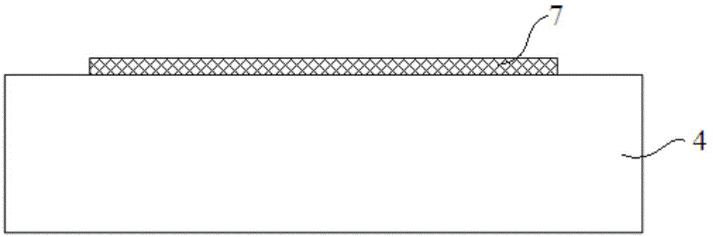
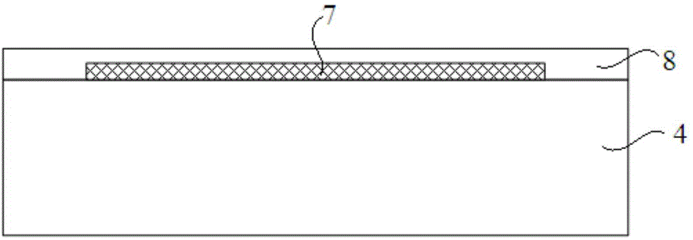
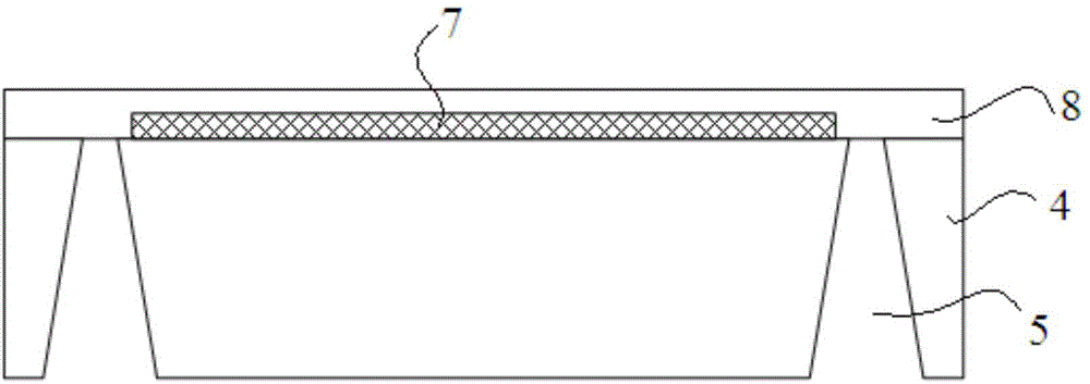
[0035] The low-frequency IPD package 2 includes a first high-resistance silicon wafer 4, a low-frequency IPD circuit 7 is set on the front of the first high-resistance silicon wafer 4, and a low-frequency IPD circuit 7 is arranged on the front of the first high-resistance silicon wafer 4. The surface is covered with a protective first passivation layer 8, and the first TSV hole 5 is formed by etching on the back of the first high-resistance silicon wafer 4, and the first TSV hole 5 is filled with the first conductive material 6. A first metal pad 9 ...


PUM


Abstract

The invention relates to a three-dimensional integrated wafer-level package structure and a package method for a high-frequency IPD (Integrated Passive Device) module. The three-dimensional integrated wafer-level package structure comprises an PCB (Printed Circuit Board) system board and is characterized in that a low-frequency IPD package body is piled on the PCB system board, and a radio-frequency IPD package body is piled on the low-frequency IPD package body; the PCB system board is connected with the front surface of the low-frequency IPD package body through a solder ball; the low-frequency IPD package body is electrically connected with the outside through a solder ball; the low-frequency IPD package body is connected with the radio-frequency IPD package body through a first metal soldering pad and a second metal soldering pad. According to the package structure and the package method, the functions of the radio-frequency IPD module are partitioned, and an IPD chip is partitioned into two parts including a lower-frequency circuit and a radio-frequency circuit; the packaging of the radio-frequency IPD module with a three-dimensional structure is realized by adopting wafer-level planar machining and TSV (Through Silicon Via) three-dimensional integrated wafer technologies based on a high-resistance silicon material, and the interference of the radio-frequency IPD module on a signal circuit on the PCB system board is reduced. In the meantime, the area of occupying the PCB system board is correspondingly reduced, and device and system minimization is facilitated.

Description

technical field [0001] The invention relates to a three-dimensional integrated wafer-level packaging structure and packaging method of a high-frequency IPD module, belonging to the technical field of IPD devices. Background technique [0002] After nearly ten years of development, IPD (Integrated Passive Devices) is gaining more and more recognition in the market. The power to promote the development of IPD mainly comes from mobile communication products. Taking the commonly used dual-band mobile phone as an example, there are about 100~300 components in the whole machine, and passive components account for 95% of the mobile phone components, and the overall 70% of the PCB area; in view of this, manufacturers' demand for IPD (Integrated Passive Devices) will continue to grow, because the use of integrated solutions is still one of the few ways to continue to reduce size and increase functionality. In the past few years, most IPD components were mainly concentrated in baseba...

Claims


Application Information

Patent Timeline
Patent Type & Authority Applications(China)
IPC IPC(8): H05K1/18H05K3/34H01L23/538H01L21/768
CPCH01L23/538H01L21/768H01L21/76838H05K1/18H05K3/34H05K2201/10
Inventor 孙鹏何洪文徐健
Owner NAT CENT FOR ADVANCED PACKAGING
Why Eureka
Try Eureka