In-situ electrochemical-surface enhanced raman scattering chip and production method thereof

A surface-enhanced Raman and in-situ electrochemical technology, which is applied in the fields of material electrochemical variables, Raman scattering, material excitation analysis, etc. Integration and other issues, to achieve the effect of high integration and miniaturization, easy fabrication and production, and reduced inspection costs

Active Publication Date: 2015-04-08
ZHEJIANG UNIV OF TECH
View PDF1 Cites 12 Cited by
  • Summary
  • Abstract
  • Description
  • Claims
  • Application Information

AI Technical Summary

Problems solved by technology

Pillar electrodes are bulky, making integration of working, counter and reference electrodes difficult
(2) The roughened surface obtained after the treatment of this type of columnar electrode on the chip, the size and distribution of nanoparticles are difficult to achieve uniformity, which makes the Raman detection signal vary greatly at different detection sites on the surface
(3) The operation process of grinding, ultrasonic cleaning, activation and oxidation-reduction reaction to obtain nanostructure or roughening of the surface of the columnar electrode before use is relatively cumbersome
(4) The cost of chips using rod-shaped noble metal electrodes is high, and it is not easy to reuse, and it is not suitable for popularization and use in portable in-situ EC-SERS.

Method used


Image

  • In-situ electrochemical-surface enhanced raman scattering chip and production method thereof
  • In-situ electrochemical-surface enhanced raman scattering chip and production method thereof
  • In-situ electrochemical-surface enhanced raman scattering chip and production method thereof

Examples


Embodiment Construction

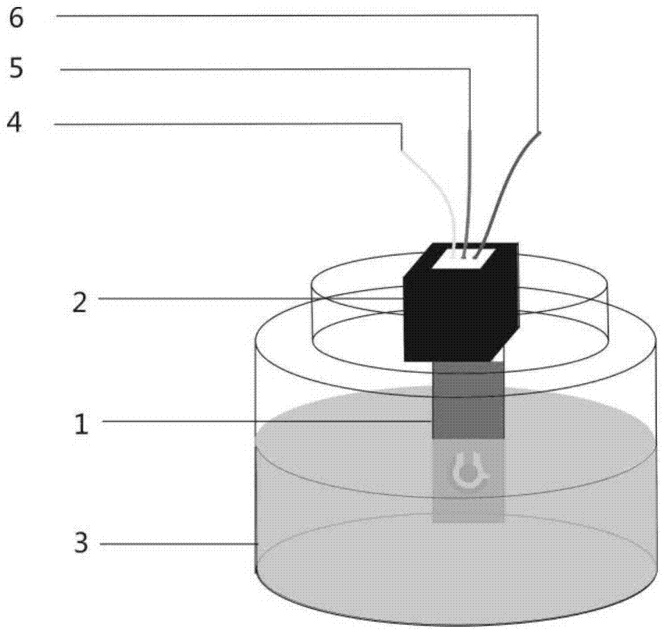
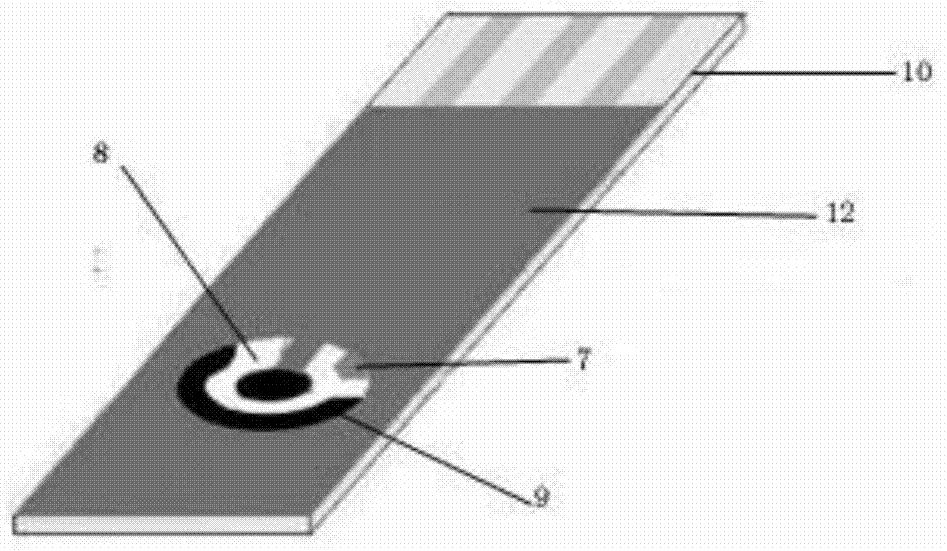
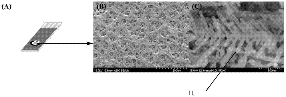
[0021] The in-situ electrochemical-surface-enhanced Raman spectroscopy chip described in this embodiment includes a substrate 10, which is a polyethylene terephthalate plate. The substrate 10 is provided with a conductive silver ink printing layer, a carbon ink printing layer, and a silver / silver chloride ink printing layer; a working electrode 8, a counter electrode 7 and a reference electrode 9 are integrated on the substrate, and the working electrode 8 and the counter electrode 7 Located on the carbon ink printing layer, the reference electrode 9 is located on the silver / silver chloride conductive ink printing layer; wherein the surface of the working electrode 8 is a porous nano-dendritic structure 11, and the surface layer of the chip is provided with a conductive end, a working electrode working end, and a counter electrode. The working end and the reference electrode working end, and other specific areas of the surface layer are insulating layers 12 . The insulating la...


PUM


Abstract

The invention discloses an in-situ electrochemical-surface enhanced raman scattering chip, which comprises a substrate. The substrate integrates a working electrode, a counter electrode and a reference electrode, wherein the working electrode surface is a nano-structure, the chip surface layer is provided with a conductive end, a working electrode working end, a counter electrode working end and a reference electrode working end, and other surface layer specific area is an insulating layer. The insulating layer separates the conductive area where the conductive end of the chip is located from the working area where the three-electrode working ends are located. According to the invention, a silk-screen printing process is employed to make the substrate, electrodeposition reaction is utilized to treat the working electrode surface, the time is short and the operation is simple and easy to control, thus being convenient for large-scale making and production. The slice chip prepared by the invention overcomes the defects of large volume and difficult integration of columnar electrodes, and realizes high degree integration and miniaturization. And after the electrodeposition reaction, the working electrode surface with a nano-structure, especially the working electrode surface with a porous nano-dendritic structure is more uniform.

Description

technical field [0001] The invention belongs to the field of Raman spectrum detection, in particular to a chip for in-situ electrochemical-surface enhanced Raman spectrum detection (Electrochemical-Surface enhanced raman scattering, EC-SERS). Background technique [0002] Electrochemical methods can provide information on the electron transfer of molecules under the action of an electric field, while Raman spectroscopy can provide information on the vibration of molecular groups. Therefore, in situ EC-SERS spectroscopy is the solution to the interface electron transfer mechanism and electrical pre-enrichment analysis. etc. powerful tool. For the working electrode on the chip of in-situ detection combined with in-situ EC-SERS, it is required that the electrode can not only provide electrical conductivity, but also have the ability to amplify the Raman detection signal by 10 after special treatment on the surface. 4 -10 6 double effect. The electrodes of the in-situ EC-SERS...

Claims


Application Information

Patent Timeline
Patent Type & Authority Applications(China)
IPC IPC(8): G01N21/65G01N27/30
Inventor 滕渊洁刘文涵
Owner ZHEJIANG UNIV OF TECH
Why Eureka
Try Eureka