Semiconductor device and formation method thereof

A semiconductor and device technology, applied in the field of semiconductor devices and their formation, can solve problems such as device damage in the storage area, achieve the effects of improving the yield rate, protecting the storage area, and expanding the etching window

Active Publication Date: 2015-04-22
SHANGHAI HUAHONG GRACE SEMICON MFG CORP
View PDF4 Cites 0 Cited by
  • Summary
  • Abstract
  • Description
  • Claims
  • Application Information

AI Technical Summary

Problems solved by technology

[0006] However, in the semiconductor device formed by the prior art, when removing the mask layer 14b of the peripheral region, the mask layer 14a of the storage region is also easily removed, so that the devices in the storage region are damaged during the manufacturing process of the peripheral circuit

Method used


Image

  • Semiconductor device and formation method thereof
  • Semiconductor device and formation method thereof
  • Semiconductor device and formation method thereof

Examples


Embodiment Construction

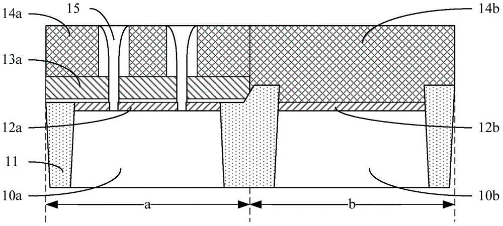
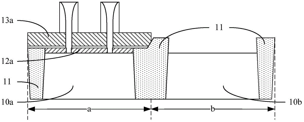
[0048] It can be seen from the background technology that when using the existing technology to form a semiconductor device, the problem of material removal of the mask layer in the storage area is prone to occur. The cause of the problem is analyzed in combination with the formation process of the device:

[0049] refer to Figure 1 to Figure 2 , when the substrate 10 is formed, the peripheral region mask layer 14b has a different thickness on the peripheral region floating gate layer 12b and the isolation structure 11, and cannot be completely removed by dry etching. Therefore, in the process of removing the mask layer 14b in the peripheral region, wet etching is often required. However, the storage area mask layer 14a and the peripheral area mask layer 14b are made of the same material. Therefore, during the process of wet etching to remove the peripheral region mask layer 14b, the storage region mask layer 14a will also be removed at the same time.

[0050] In order to so...


PUM

PropertyMeasurementUnit
Width rangeaaaaaaaaaa

Abstract

The invention discloses a semiconductor device and a formation method of the semiconductor device. The method comprises the steps that a substrate is provided, and the substrate comprises a storage area and a periphery area; a storage area masking layer is formed on the substrate of the storage area; a protection ring wrapping the storage area masking layer is formed on the substrate of the storage area; the substrate of the periphery area is provided with a periphery area floating barrier layer and a periphery area masking layer in sequence; protection layers are formed on the storage area masking layer, the protection ring and the periphery area masking layer, wherein the protection layer in the storage area is the storage area protection layer, and the protection layer in the periphery area is the periphery area protection layer; the periphery area protection layer, the periphery area masking layer and the periphery area floating barrier layer are sequentially removed, and the substrate of the periphery area is revealed. According to semiconductor device and the formation method of the semiconductor device, by the arrangement of the protection layer and the protection ring surrounding the storage area, the storage area can be protected when an upper film layer of the substrate of the periphery area is removed, the storage area can be protected from the impact of the periphery area etching technique, the etching process window of the periphery area can be effectively enlarged, the yield of device manufacturing can be improved, and the cost of device manufacturing can be reduced.

Description

technical field [0001] The invention relates to the field of semiconductor manufacturing, in particular to a semiconductor device and a forming method thereof. Background technique [0002] The etching process is one of the commonly used processes in the field of semiconductor manufacturing. In the etching process, photoresist is often used as a mask. However, with the gradual reduction of the size of semiconductor devices, it is easy to cause light scattering during exposure, so that the formed photoresist pattern is deviated from the original design. Therefore, more hard masks are used in semiconductor etching, the hard masks are etched using photoresist as a mask, and then devices are formed by etching using the hard mask as a mask. After the device is formed, the hard mask is removed. [0003] refer to Figure 1 to Figure 2 , shows a schematic diagram of a method for forming a semiconductor device in the prior art. Here, the formation of an embedded flash memory is t...

Claims


Application Information

Patent Timeline
IPC IPC(8): H01L21/8247H01L27/115
CPCH10B41/00H10B41/30
Inventor 高超王哲献江红李冰寒
Owner SHANGHAI HUAHONG GRACE SEMICON MFG CORP
Why Eureka
Try Eureka