
Single-stage boost inverter

An inverter, single-stage technology, applied in the field of single-stage boost inverter, can solve the problems of high busbar cost and large loss, and achieve the effects of low cost, low loss and simple method

Active Publication Date: 2015-04-29
NANJING UNIV OF AERONAUTICS & ASTRONAUTICS
View PDF2 Cites 7 Cited by
  • Summary
  • Abstract
  • Description
  • Claims
  • Application Information

AI Technical Summary

Problems solved by technology

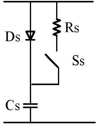
In this way, the resistor only consumes energy when it is not straight through, but for a single-stage boost inverter with high power and high current, this part of the loss is very large, so this absorption circuit is only suitable for single-stage boost inverters with small and medium power. voltage inverter
[0005] For medium and high-power inverters, traditional inverters usually use busbars to reduce the distributed inductance of the DC busbar and reduce the voltage peak of the DC busbar, but the cost of the busbar is relatively high

Method used


Image

  • Single-stage boost inverter
  • Single-stage boost inverter
  • Single-stage boost inverter

Examples


Embodiment Construction

[0049] Below in conjunction with accompanying drawing, technical scheme of the present invention is described in further detail:

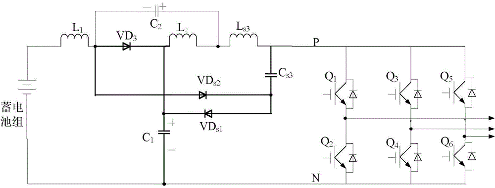
[0050] Such as image 3 As shown, the present invention discloses a single-stage boost inverter, which includes a battery pack, inductor L1, inductor L2, inductor Ls3, capacitor C1, capacitor Cs3, capacitor C2, diode VDs1, diode VDs2 and diode VD3, wherein , the inductance Ls3 is a parasitic inductance, and the diode VDs1, diode VDs2 and diode VD3 are all fast recovery diodes; one end of the inductance L1 is connected to the positive pole of the battery pack, and the other end is respectively connected to one end of the capacitor C2, the anode of the diode VD3, and the diode VDs2 The other end of the capacitor C2 is connected to one end of the inductor L2 and one end of the inductor Ls3; the cathode of the diode VD3 is connected to the other end of the inductor L2, the cathode of the diode VDs1, and one end of the capacitor C1; the other end of the...


PUM


Abstract

The invention discloses a single-stage boost inverter. By taking full advantages of a distributed inductor and a parasitic inductor, the distributed inductor, the parasitic inductor and an external capacitor form a passive network and are participated in the working condition of the single-stage boost inverter. According to the single-stage boost inverter with medium and high power, when the through vector state of the single-stage boost inverter is converted into a non-through state, distributed inductance and parasitic inductance exist in a direct current bus link, and then extremely high voltage spike can be generated on a direct current bus of the inverter, so that a power tube is easy to burn out. In order to improve the reliability of the inverter, a stage of suppression circuit is needed to be added. A stage of suppression circuit does not need to be specially added to the single-stage boost inverter disclosed by the invention, and the single-stage boost inverter is suitable for lower power levels and also suitable for higher power levels.

Description

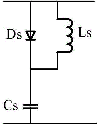
technical field [0001] The invention relates to an inverter, in particular to a single-stage boost inverter with the function of suppressing a DC bus voltage spike. Background technique [0002] The single-stage boost inverter (Z-source inverter, quasi-Z-source inverter) has three working modes: through zero-vector state, effective vector state, and open-circuit zero-vector state. [0003] Due to the distributed inductance and parasitic inductance in the DC bus link, when the single-stage boost inverter is switched from the through state to the non-through state, the DC bus voltage has a high voltage spike, which is very easy to damage the power device. [0004] In order to absorb the voltage spike on the DC bus, a suppression circuit must be added, such as figure 1 As shown, in order to solve the traditional RC, RCD, RCD limiter snubber circuit in the single-stage boost inverter, the DC bus voltage is too high and the loss is too large, and the LCD snubber circuit will osc...

Claims


Application Information

Patent Timeline
Patent Type & Authority Applications(China)
IPC IPC(8): H02M7/5387H02M1/32
CPCH02M1/32H02M7/5387H02M1/0038
Inventor 李春杰黄文新
Owner NANJING UNIV OF AERONAUTICS & ASTRONAUTICS
Learn More