MEMS process based miniature packaged F-P pressure sensor and forming method

A pressure sensor, F-P technology, which is applied in fluid pressure measurement using optical methods, and measurement of the change force of optical properties of materials when they are stressed, can solve low detection sensitivity, difficulty in making microgrooves, and two F-P chambers. problems such as poor parallelism of each end face, to achieve high resolution, avoid detection accuracy and resolution reduction, and take into account the effect of measurement accuracy

Active Publication Date: 2015-05-06
SHANGHAI BAIANTEK SENSING TECH CO LTD
View PDF6 Cites 12 Cited by
  • Summary
  • Abstract
  • Description
  • Claims
  • Application Information

AI Technical Summary

Problems solved by technology

There are many defects in the existing all-fiber F-P pressure sensor, such as polishing the end face of the connected optical fiber, the quality of the polishing is poor, and it is difficult to make the microgroove, so that the roughness of the two end faces of the F-P cavity is relatively high. Poor, and it is difficult to deposit a high reflection film on the end face; two optical fibers are welded, and the parallelism of the two end faces of the F-P cavity is poor, which makes the existing F-P pressure sensor difficult to manufacture, the signal-to-noise ratio of the detection signal is poor, and the detection sensitivity is low inferior

Method used


Image

  • MEMS process based miniature packaged F-P pressure sensor and forming method
  • MEMS process based miniature packaged F-P pressure sensor and forming method
  • MEMS process based miniature packaged F-P pressure sensor and forming method

Examples


Embodiment

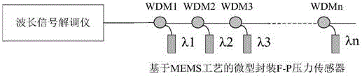
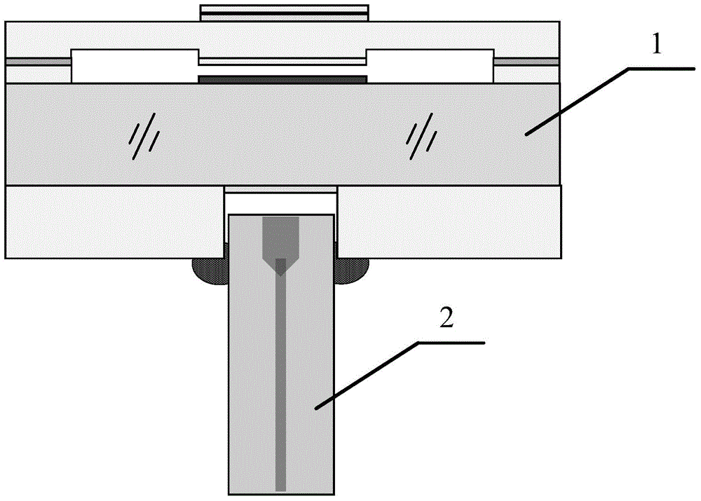
[0056] A schematic diagram of the structure of a micro-encapsulated F-P pressure sensor based on MEMS technology is shown in figure 1 As shown, the F-P pressure sensor mainly includes a F-P pressure-sensitive MEMS chip 1 and a collimated beam expanding optical fiber 2;

[0057] Wherein, the structure diagram of F-P pressure-sensitive MEMS chip 1 is as follows figure 2 As shown, the F-P pressure-sensitive MEMS chip 1 is composed of an SOI silicon wafer, a glass wafer 3 and a double-thrown silicon wafer 4;

[0058] The SOI silicon wafer includes a top layer of silicon 5, an intermediate oxide layer 6 and a bottom layer of silicon 7; wherein, the upper surface of the bottom layer of silicon 7 is deposited with an anti-reflection film 8 and a passivation layer 10; the lower surface of the bottom layer of silicon 7 is provided with an annular groove And the circular protrusion, the circular protrusion is located in the center of the annular groove, forming a "membrane-island" str...


PUM

PropertyMeasurementUnit
depthaaaaaaaaaa
thicknessaaaaaaaaaa
reflectanceaaaaaaaaaa

Abstract

The invention discloses an MEMS process based miniature packaged F-P pressure sensor and belongs to the field of high-accuracy optical fiber sensing measurement. The F-P pressure sensor mainly comprises an F-P strain sensitive MEMS chip and a collimation and beam expanding optical fiber, wherein the F-P strain sensitive MEMS chip consists of an SOI silicon wafer, a glass sheet and a double-parabolic silicon wafer. The SOI silicon wafer comprises top layer silicon, a middle oxidization layer and bottom layer silicon. The SOI silicon wafer is fixed the glass sheet through silicon-glass anodic bonding. The glass sheet is fixed to the double-parabolic silicon wafer through silicon-glass anodic bonding. The collimation and beam expanding optical fiber is fixed in a through hole formed in the double-parabolic silicon wafer through a welding flux. The F-P strain sensitive MEMS chip is prepared based on an MEMS micromachining technology, the F-P strain sensitive MEMS chip and the collimation and beam expanding optical fiber are aligned and packaged to form the F-P pressure sensor, and miniaturized and batch manufacture of the strain gauge can be achieved. The MEMS process based miniature packaged F-P pressure sensor is high in flexibility and measurement accuracy, excellent in over-range capacity, high in mechanical reliability and good in dynamic measurement response characteristic.

Description

technical field [0001] The invention relates to a micro-encapsulation F-P pressure sensor and a molding method based on MEMS technology, belonging to the field of high-precision optical fiber sensing and measurement. Background technique [0002] Pressure sensor is the most commonly used sensor in industrial practice and instrumentation control. The traditional pressure sensor is mainly a mechanical structural device that indicates the pressure by the deformation of the elastic element. This kind of device is bulky and heavy, and cannot provide electrical output. With the development of semiconductor technology, semiconductor pressure sensors also emerge as the times require, especially with the development of MEMS technology, semiconductor sensors are developing towards miniaturization and low power consumption. [0003] MEMS pressure sensors that use electrical signal detection are mainly piezoresistive and capacitive. Piezoresistive pressure sensors refer to sensors made...

Claims


Application Information

Patent Timeline
Patent Type & Authority Applications(China)
IPC IPC(8): G01L1/24G01L11/02
Inventor 刘玉珏
Owner SHANGHAI BAIANTEK SENSING TECH CO LTD
Why Eureka
Try Eureka