Multi-die high-power diode shell and manufacturing method thereof as well as chip packaging method

A high-power diode and multi-die technology, applied in semiconductor/solid-state device manufacturing, electrical components, electric solid-state devices, etc., can solve the problems of low flexibility, low reliability, and high cost, and achieve reliable mechanical strength and heat dissipation performance Excellent, excellent heat dissipation effect

Inactive Publication Date: 2015-05-06
NO 55 INST CHINA ELECTRONIC SCI & TECHNOLOGYGROUP CO LTD
View PDF5 Cites 8 Cited by
  • Summary
  • Abstract
  • Description
  • Claims
  • Application Information

AI Technical Summary

Problems solved by technology

Even if multiple chips are packaged in one shell, there are problems of high cost, low reliability, and low flexibility

Method used


Image

  • Multi-die high-power diode shell and manufacturing method thereof as well as chip packaging method
  • Multi-die high-power diode shell and manufacturing method thereof as well as chip packaging method

Examples


Embodiment 1

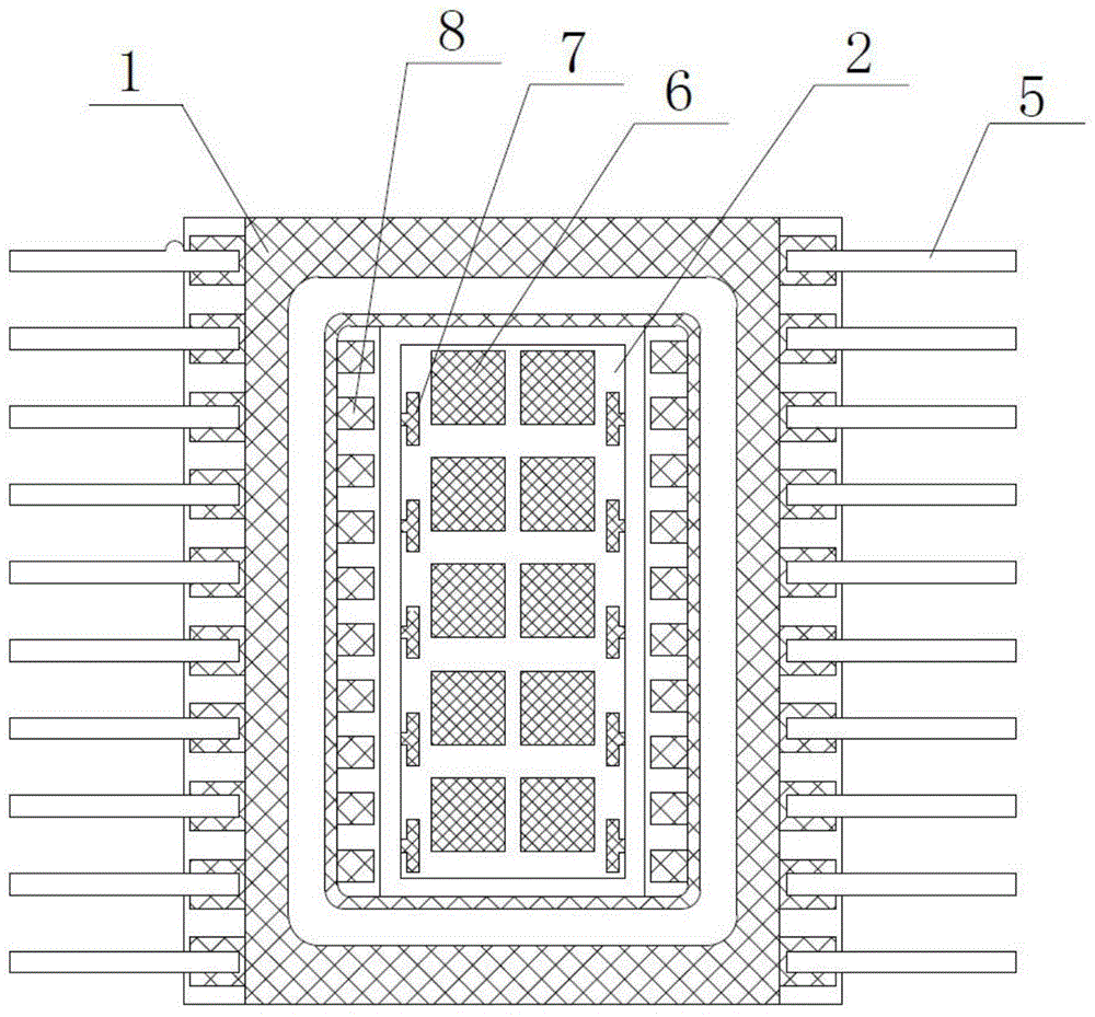
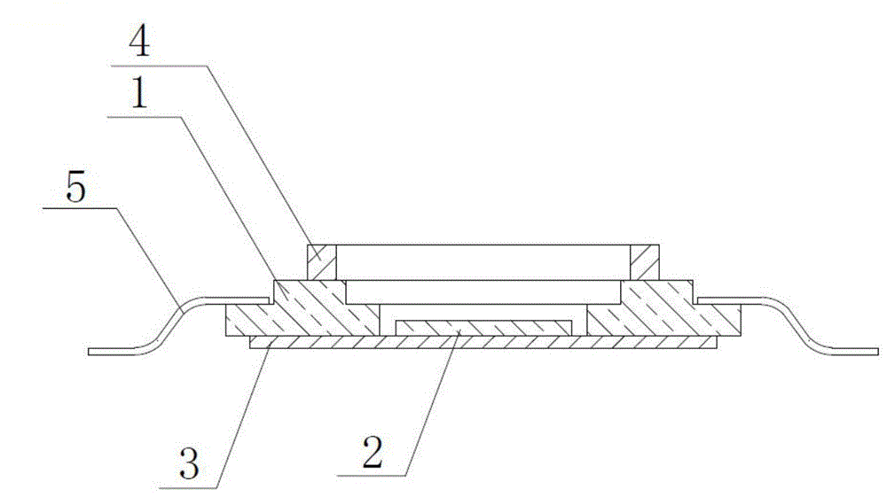
[0045] The preparation method of the multi-tube-core high-power diode casing of the present invention adopts high-temperature co-fired ceramic production technology and brazing technology. On the precise and dense AlN raw ceramic tape with a size of 180mm×180mm×0.2mm, the required circuit pattern and solderable metallization layer are produced by using precision conductive paste printing, blocking paste printing and other processes, and precision printed wiring The minimum line width is 100μm, and the minimum wiring spacing is 150μm; use laser cavity opening, lamination and other processes to produce green ceramic sheets with specific cavities and shapes; use high-precision temperature-controlled furnaces to sinter at high temperatures under certain sintering process conditions. Shaped high-temperature co-fired ceramic substrate and ceramic frame; the interconnection between ceramic components and metal components is realized through brazing technology, and a high-reliability s...


PUM

PropertyMeasurementUnit
thicknessaaaaaaaaaa

Abstract

The invention discloses a multi-die high-power diode shell and a manufacturing method thereof as well as a chip packaging method. The multi-die shell comprises a ceramic frame and a substrate; a plurality of microstrip lines are put through the frame; a first bonding region is arranged on the inner side of the frame, while a plurality of leads are arranged on the outer side of the frame; the substrate is arranged at the bottom of the inner side of the ceramic frame, and provided with a ceramic base body, and an upper side surface and a lower side surface for metallizing the ceramic base body; a plurality of isolation regions and a second bonding region are formed on the upper side surface; the isolation regions are used for receiving the chip. According to the manufacturing method, a high-temperature cofiring ceramic process is adopted, and high-heat dissipation and high-reliability multi-die packaging is realized by virtue of a structure in which a metal heat sink is brazed under the chip substrate and a kovar weld ring is brazed and sealed on the upper surface of the ceramic frame, and meanwhile, the requirements of large current and high power property are achieved.

Description

technical field [0001] The invention relates to the technical field of semiconductor chip packaging, in particular to a multi-core high-power diode shell, a manufacturing method thereof, and a chip packaging method. Background technique [0002] At present, most of the diode packaging shells are low-current or single-chip low-power shells, which are difficult to meet the market's development trend of miniaturization, integration, high current, high power, and high reliability of diodes. Ceramic-metal packaging components are a good combination of these trending factors. Because of their advantages of miniaturization, high reliability, and excellent electrical and thermal performance, they have gained more and more applications in the diode packaging industry. One of the development trends of diode packaging components. [0003] Traditional ceramic-metal package-based diode chip housings mainly adopt single-chip packaging, that is to say, only one chip is packaged in a ceram...

Claims


Application Information

Patent Timeline
Patent Type & Authority Applications(China)
IPC IPC(8): H01L23/02H01L23/367H01L21/50H01L21/60H01L23/488H01L21/56
Inventor 郭怀新程凯胡进王子良
Owner NO 55 INST CHINA ELECTRONIC SCI & TECHNOLOGYGROUP CO LTD
Why Eureka
Try Eureka