A trench mosfet structure and method of making the same

A manufacturing method and trench technology, which are applied in semiconductor/solid-state device manufacturing, semiconductor devices, electrical components, etc., can solve the problem of low withstand voltage capacity in the terminal area, increase the degree of depletion, improve the withstand voltage capacity, and improve The effect of pressure resistance

Active Publication Date: 2019-02-26
WUXI TONGFANG MICROELECTRONICS
View PDF6 Cites 0 Cited by
  • Summary
  • Abstract
  • Description
  • Claims
  • Application Information

AI Technical Summary

Problems solved by technology

[0007] In view of the above-mentioned shortcomings of the prior art, the purpose of the present invention is to provide a trench MOSFET structure and its manufacturing method, which is used to solve the problem of low withstand voltage capability of the terminal region of the trench MOSFET structure in the prior art

Method used


Image

  • A trench mosfet structure and method of making the same
  • A trench mosfet structure and method of making the same
  • A trench mosfet structure and method of making the same

Examples


Embodiment 1

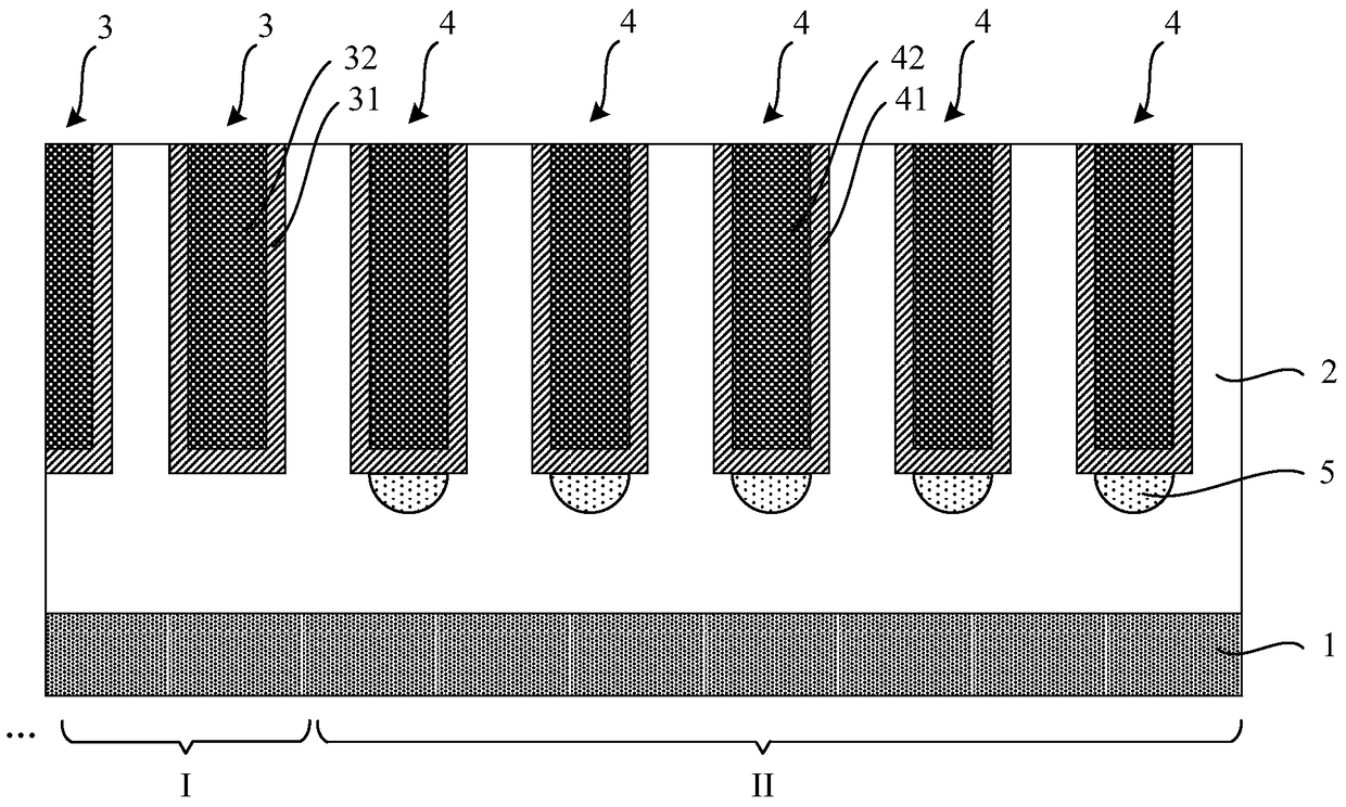
[0052] The present invention provides a trench MOSFET structure, please refer to figure 1, showing a cross-sectional view of the structure, including an N-type heavily doped substrate 1 and an N-type lightly doped epitaxial layer 2 formed on the N-type heavily doped substrate 1; the N-type lightly doped epitaxial layer Several trench structures 3 in the cell region and several trench structures 4 in the termination region are formed in 2, wherein at least one trench structure 4 in the termination region is connected to a P-type doped structure 5 at its bottom.

[0053] The cell region trench structure 3 is located in the cell region I of the trench MOSFET structure, and the termination region trench structure 4 is located in the termination region II of the trench MOSFET structure.

[0054] Specifically, the N-type heavily doped substrate 1 serves as the drain region of the trench MOSFET structure, and the N-type lightly doped epitaxial layer 2 serves as the drift region of th...

Embodiment 2

[0060] This embodiment adopts basically the same technical solution as Embodiment 1, the difference is that in Embodiment 1, the trench structure in the cell area adopts a conventional trench gate structure, while in this embodiment, the trench structure in the cell area The structure adopts the split gate structure.

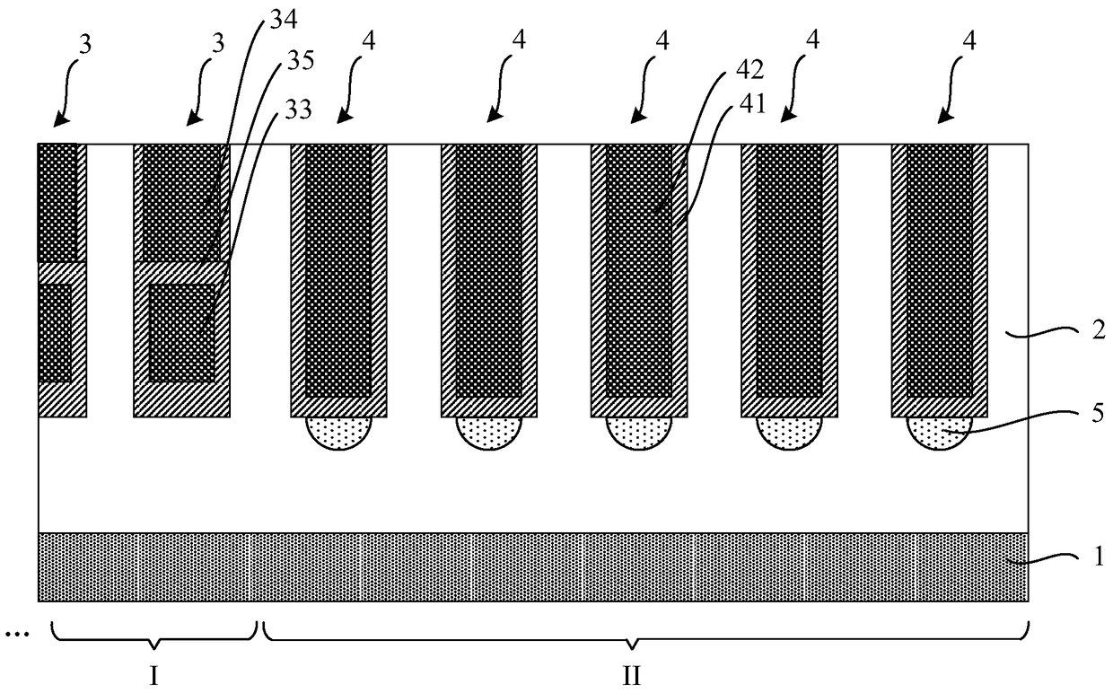
[0061] see figure 2 , showing a cross-sectional view of a trench MOSFET structure in this embodiment, including an N-type heavily doped substrate 1 and an N-type lightly doped epitaxial layer 2 formed on the N-type heavily doped substrate 1; the N A plurality of cell region trench structures 3 and a plurality of termination region trench structures 4 are formed in the lightly doped epitaxial layer 2, wherein at least one termination region trench structure 4 is connected to a P-type doping structure 5 at its bottom.

[0062] Such as figure 2 As shown, the cell region trench structure 3 is a split gate, including a shielding gate 33 and a control gate 34 form...

Embodiment 3

[0066] A kind of fabrication method of trench MOSFET structure of the present invention is as follows, at least comprises the following steps:

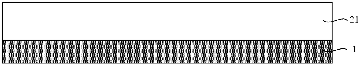
[0067] See first image 3 , performing step S1: providing an N-type heavily doped substrate 1 , and epitaxially first N-type lightly doped layer 21 on the N-type heavily doped substrate 1 .

[0068] The N-type heavily doped substrate 1 serves as the drain region of the trench MOSFET structure, and the N-type lightly doped epitaxial layer 1 serves as a part of the drift region of the trench MOSFET structure.

[0069] then see Figure 4 and Figure 5 , perform step S2: perform P-type ion implantation, and form at least one P-type doped structure 5 on the upper part of the first N lightly doped layer 21; corresponding to the location.

[0070] Specifically, such as Figure 4 As shown, firstly a mask layer 6 is formed on the surface of the first N-type lightly doped layer 21, and at least one opening 7 is formed in the mask layer 6, ...


PUM


Abstract

The invention provides a trench MOSFET structure and a manufacturing method thereof. The structure includes an N-type heavy doped substrate and an N-type light doped epitaxial layer formed on the N-type heavy doped substrate, wherein a plurality of cellular area trench structures and a plurality of terminal area trench structures are formed in the N-type light doped epitaxial layer, and the bottom of at least one terminal area trench structure is connected with a P-type doping structure. The P-type doping structure can reduce the N-type doping density of the area the P-type doping structure is located, and thereby the consumption degree of the area when the device works is increased, and promotion of the pressure-resistant capacity of the medium-pressure MOSFET terminal area is facilitated.

Description

technical field [0001] The invention belongs to the field of electronic devices, and relates to a trench MOSFET structure and a manufacturing method thereof. Background technique [0002] For semiconductor devices commonly used in power electronic systems and power management, the power Metal-Oxide-Semiconductor-Field-Effect-Transistor MOSFET (Metal-Oxide-Semiconductor-Field-Effect-Transistor), or Insulated Gate Field-Effect Transistor, is widely introduced . [0003] Trench power MOSFET is a new high-efficiency and power switching device developed after MOSFET. It adopts trench gate structure field effect transistor, which not only inherits the high input impedance of MOS field effect transistor (≥10 8 Ω), small driving current (about 0.1μA), and also has excellent characteristics such as high withstand voltage, large working current, high output power, good transconductance, and fast switching speed. It is precisely because it combines the advantages of electron tubes an...

Claims


Application Information

Patent Timeline
Patent Type & Authority Patents(China)
IPC IPC(8): H01L29/78H01L29/06H01L21/336
CPCH01L29/0684H01L29/66477H01L29/78
Inventor 白玉明刘锋张海涛
Owner WUXI TONGFANG MICROELECTRONICS
Why Eureka
Try Eureka