
A bandwidth-compensated ultra-high-speed laser driver circuit and driver chip
A laser driver and ultra-high-speed technology, used in lasers, laser parts, semiconductor lasers, etc., can solve the problems of increasing chip cost, occupying a large chip area, complex structure, etc., to expand the bandwidth and eliminate the effect of parasitic capacitance.
Patent Information
- Authority / Receiving Office
- CN · China
- Patent Type
- Patents(China)
- Current Assignee / Owner
- Publication Date
- 2017-06-16
Smart Images
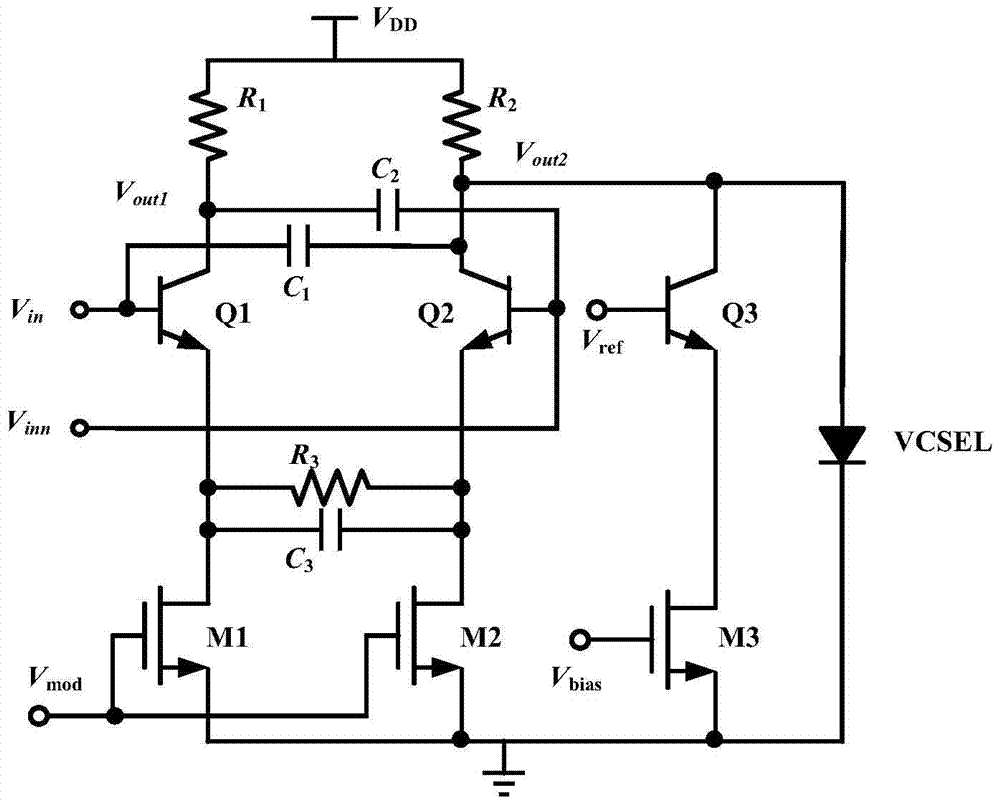
Figure 1 
Figure 2
Abstract
Description
Technical field
[0001] The invention relates to a laser driver circuit at the transmitting end in a system such as optical fiber communication, and in particular to a bandwidth compensated ultra-high-speed laser driver circuit and a driver chip. Background technique
[0002] The optical fiber communication system has developed rapidly in network and multimedia communication due to its large capacity and other characteristics. The front end of the optical fiber is the light emitting end, which is composed of a multiplexer, a laser driver and a laser diode. The function of the optical transmitter is to multiplex multiple low-speed data signals into a high-speed signal through the multiplexer. After being amplified by the laser driver circuit, the laser diode is driven to emit light, converted into high-speed optical signals, and transmitted through optical fibers. Therefore, the design goal of the laser driver is to obtain high bandwidth and large output modulation swing performan...
Examples
Embodiment Construction
[0024] In the following, the present invention will be further explained in conjunction with the embodiments.
[0025] Such as figure 1 As shown, in the ultra-high-speed laser driver circuit for bandwidth compensation in this embodiment, the connections of various components are as follows:
[0026] The base of the NPN bipolar transistor Q1 is connected to the input voltage V in And capacitance C 1 The first terminal of the transistor Q1 is connected to the resistor R 1 The first terminal and the capacitor C 2 On the first end, the emitter of transistor Q1 is connected to the drain of MOS transistor M1 on the one hand, and resistor R on the other hand 3 The first terminal and the capacitor C 3 The first end of
[0027] The base of the NPN bipolar transistor Q2 is connected to the input voltage V inn And capacitance C 2 The second terminal of the transistor Q2 is connected to the resistor R 2 The first terminal, capacitor C 1 The second terminal of the transistor Q3, the collector o...