Preparation method for copper substrate for vertical LED (light-emitting diode) chips

An LED chip, vertical structure technology, applied in electrical components, circuits, semiconductor devices, etc., can solve the problems of high cost, complicated preliminary preparation, hinder the industrialization of vertical structure LED, etc., to improve the yield and overcome a large number of copper adhesion. , the effect of low cost of preparation

Active Publication Date: 2015-05-20
广州市众拓光电科技有限公司
View PDF2 Cites 2 Cited by
  • Summary
  • Abstract
  • Description
  • Claims
  • Application Information

AI Technical Summary

Problems solved by technology

However, bonding copper has very strict requirements on experimental conditions, such as temperature and pressure, and requires a metal transition layer for bonding. It faces problems such as complicated preparations and high costs, which largely hinder the industrialization of vertical structure LEDs.

Method used


Image

  • Preparation method for copper substrate for vertical LED (light-emitting diode) chips
  • Preparation method for copper substrate for vertical LED (light-emitting diode) chips
  • Preparation method for copper substrate for vertical LED (light-emitting diode) chips

Examples


Embodiment 1

[0036] The preparation method of the copper substrate for the vertical structure LED chip of the present embodiment comprises the following steps:

[0037] The preparation method for the copper base plate of vertical structure LED chip is characterized in that, comprises the following steps:

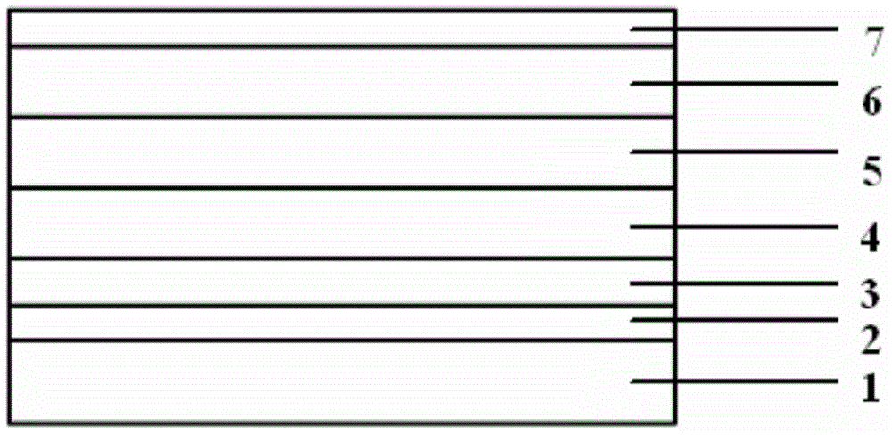
[0038] 1) Evaporate a P-type metal electrode layer on the surface of the GaN epitaxial wafer, the metal in the P-type metal electrode layer is Cr or Pt, and then plate a P-type metal electrode layer on the P-type metal electrode layer by using photolithography or evaporation technology. layer Au to obtain the first substrate; the thickness of the Cr or Pt is 30-50nm, and the thickness of the Au is 800-1000nm.

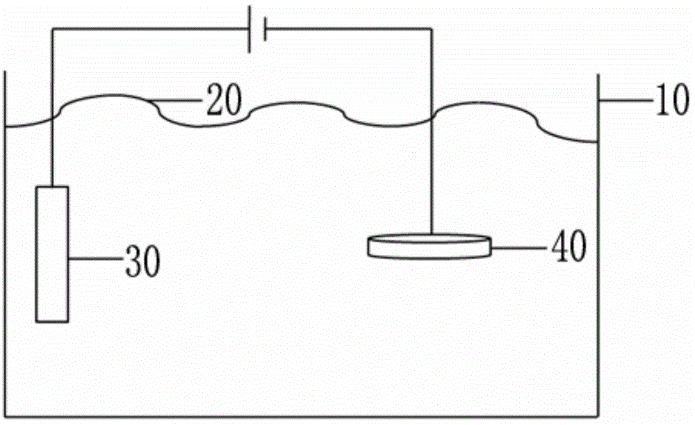
[0039] 2) The first substrate is cleaned, and after the degreasing effect is achieved, the concentration is 10% H 2 SO 4 Surface activation was performed for 1 min; the specific process of cleaning was 1.5, 1.5, and 1 min with acetone, ethanol, and deionized water, respectively....

Embodiment 2

[0051] The preparation method for the copper substrate of the vertical structure LED chip described in this embodiment comprises the following steps:

[0052] 1) Evaporate a P-type metal electrode layer on the surface of the GaN epitaxial wafer, the metal in the P-type metal electrode layer is Cr or Pt, and then plate a P-type metal electrode layer on the P-type metal electrode layer by using photolithography or evaporation technology. layer Au to obtain the first substrate; the thickness of the Cr or Pt is 30nm, and the thickness of the Au is 1000nm.

[0053] 2) The first substrate is cleaned, and after the degreasing effect is achieved, the concentration is 10% H 2 SO 4 Surface activation was performed for 1 min; the specific process of cleaning was 1.5, 1.5, and 1 min with acetone, ethanol, and deionized water, respectively.

[0054] 3) Blacken the phosphorus copper anode containing 0.04wt% phosphorus for 3 hours, and then clean it; the cleaning solution used in the clean...

Embodiment 3

[0062] The preparation method for the copper substrate of the vertical structure LED chip described in this embodiment comprises the following steps:

[0063] 1) Evaporate a P-type metal electrode layer on the surface of the GaN epitaxial wafer, the metal in the P-type metal electrode layer is Cr or Pt, and then plate a P-type metal electrode layer on the P-type metal electrode layer by using photolithography or evaporation technology. layer Au to obtain the first substrate; the thickness of the Cr or Pt is 50nm, and the thickness of the Au is 900nm.

[0064] 2) The first substrate is cleaned, and after the degreasing effect is achieved, the concentration is 10% H 2 SO 4 Surface activation was performed for 1 min; the specific process of cleaning was 1.5, 1.5, and 1 min with acetone, ethanol, and deionized water, respectively.

[0065] 3) Blacken the phosphorus copper anode containing 0.065wt% phosphorus for 5h, and then clean it; the cleaning solution used in the cleaning p...


PUM

PropertyMeasurementUnit
thicknessaaaaaaaaaa
thicknessaaaaaaaaaa
thicknessaaaaaaaaaa

Abstract

The invention provides a preparation method for a copper substrate for vertical LED (light-emitting diode) chips, which includes the following steps: (1) a P-type metal electrode layer is deposited on the surface of an epitaxial wafer, a layer of Au is then plated on the P-type metal electrode layer, and thereby a first substrate is obtained; (2) the first substrate is cleaned, and after a degreasing effect is achieved, H2SO4 is used for surface activation; (3) a phosphorized copper anode is blackened, and is then cleaned; (4) the first substrate treated in step 2 and the phosphorized copper anode treated in step 3 are put into copper plating solution and electroplated, so that an electroplated sample is obtained; (5) the electroplated sample is cleaned in order to remove residual copper plating solution, so that the copper substrate is obtained. The preparation method has the characteristics of simple process and low preparation cost, moreover, the copper substrate prepared by the method has the characteristics of no burrs, good surface uniformity, good smoothness, low roughness and good thermal and electric conductivities, and thereby a chip which is prepared by adopting the copper substrate has high light extraction efficiency.

Description

technical field [0001] The invention relates to a method for preparing a copper substrate, in particular to a method for preparing a copper substrate for a vertical LED chip. Background technique [0002] Light-emitting diode (LED), as a new type of solid-state lighting source and green light source, has outstanding features such as small size, low power consumption, environmental protection, long service life, high brightness, low heat and colorful, and is widely used in outdoor lighting, commercial lighting and decoration Engineering and other fields have a wide range of applications. In the field of lighting, the application of LED lighting products is attracting the attention of the world. [0003] At present, Si substrate LED chips have been gradually industrialized. However, since the Si substrate itself has a light absorption rate of 90%, which greatly reduces the light extraction efficiency of the LED chip; at the same time, the thermal conductivity of the Si subst...

Claims


Application Information

Patent Timeline
Patent Type & Authority Applications(China)
IPC IPC(8): H01L33/62C25D3/38C25D5/54
CPCC25D3/38C25D5/54H01L33/62H01L33/647
Inventor 李国强
Owner 广州市众拓光电科技有限公司
Why Eureka
Try Eureka