n-type ldmos device and process method

A device, N-type technology, applied in the direction of semiconductor devices, semiconductor/solid-state device manufacturing, electrical components, etc., can solve problems such as unfavorable breakdown voltage, achieve the effect of improving potential distribution, uniform electric field distribution, and increasing breakdown voltage

Active Publication Date: 2018-06-19
SHANGHAI HUAHONG GRACE SEMICON MFG CORP
View PDF4 Cites 0 Cited by
  • Summary
  • Abstract
  • Description
  • Claims
  • Application Information

AI Technical Summary

Problems solved by technology

This structure has a high electric field strength at the drain end, which is not conducive to the improvement of the breakdown voltage BV

Method used


Image

  • n-type ldmos device and process method
  • n-type ldmos device and process method
  • n-type ldmos device and process method

Examples


Embodiment Construction

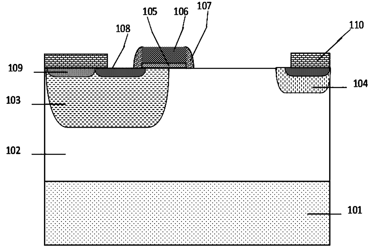
[0023] The N-type LDMOS device described in the present invention, such as Figure 8 As shown, there are P wells 103 and N wells 104 in the N-type deep wells 102 on the P-type substrate 101, and the substrate surface has polysilicon gates 106 and sidewall structures 107; there are LDMOS devices in the N wells 104 Drain region 111, there is a metal electrode 110 on the drain region 111 to lead the drain region 111; the P well 103 has a source region 108 of an LDMOS device, and a heavily doped P-type region 109, and the metal electrode will heavily dope the P-type region 109 and the source region 108 are drawn; the surface of the LDMOS device is a non-planar stepped structure, the position of the drain region is higher than the channel of the LDMOS, and the height difference h on both sides is

[0024] In order to solve the above problems, the process method of the N-type LDMOS device of the present invention comprises the following process steps:

[0025] Step 1, on the P-ty...


PUM


Abstract

The invention discloses an N type LDMOS (laterally diffused metal oxide semiconductor) device. According to the N type LDMOS device, a P well and an N well are arranged in an N type deep well on a P type substrate, and a polycrystalline silicon gate and a side wall structure are arranged on the silicon surface; a drain region of the LDMOS device is arranged in the N well and is led out by a metal electrode on the drain region; a source region of the LDMOS device and a heavily-doped P type region are arranged in the P well and are led out by the metal electrode; the surface of the LDMOS device adopts a non-planar stepped structure, and the drain region is higher than a channel of the LDMOS. The invention further discloses a processing method of the N type LDMOS device.

Description

technical field [0001] The invention relates to the field of semiconductors, in particular to an N-type LDMOS device, and also relates to a process method for the N-type LDMOS device. Background technique [0002] DMOS is currently widely used in power management circuits due to its high voltage resistance, high current drive capability and extremely low power consumption. In the BCD process, although DMOS and CMOS are integrated in the same chip, due to the requirements of high withstand voltage and low on-resistance, the conditions of DMOS in the background area and drift area are shared with the existing process conditions of CMOS. , there is a contradiction between the on-resistance and the breakdown voltage, which often cannot meet the requirements of the switch tube application. In LDMOS devices, on-resistance is an important indicator. Therefore, in order to make high-performance LDMOS, it is necessary to adopt various methods to optimize the on-resistance and break...

Claims


Application Information

Patent Timeline
Patent Type & Authority Patents(China)
IPC IPC(8): H01L29/78H01L21/336
CPCH01L29/0607H01L29/0684H01L29/0882H01L29/66681H01L29/7816
Inventor 石晶钱文生
Owner SHANGHAI HUAHONG GRACE SEMICON MFG CORP
Why Eureka
Try Eureka