Check patentability & draft patents in minutes with Patsnap Eureka AI!

Preparation method of silica-based laminated solar cell

A solar cell and stacking technology, applied in the field of solar cells, can solve the problems of low solar energy conversion efficiency of solar cells, and achieve the effects of good compatibility and low development cost

Inactive Publication Date: 2015-05-27
NANTONG UNIVERSITY
View PDF3 Cites 0 Cited by
  • Summary
  • Abstract
  • Description
  • Claims
  • Application Information

AI Technical Summary

Problems solved by technology

But the solar energy conversion efficiency of this kind of solar cell is on the low side, needs further improvement

Method used


Image

  • Preparation method of silica-based laminated solar cell
  • Preparation method of silica-based laminated solar cell
  • Preparation method of silica-based laminated solar cell

Examples


Embodiment 1

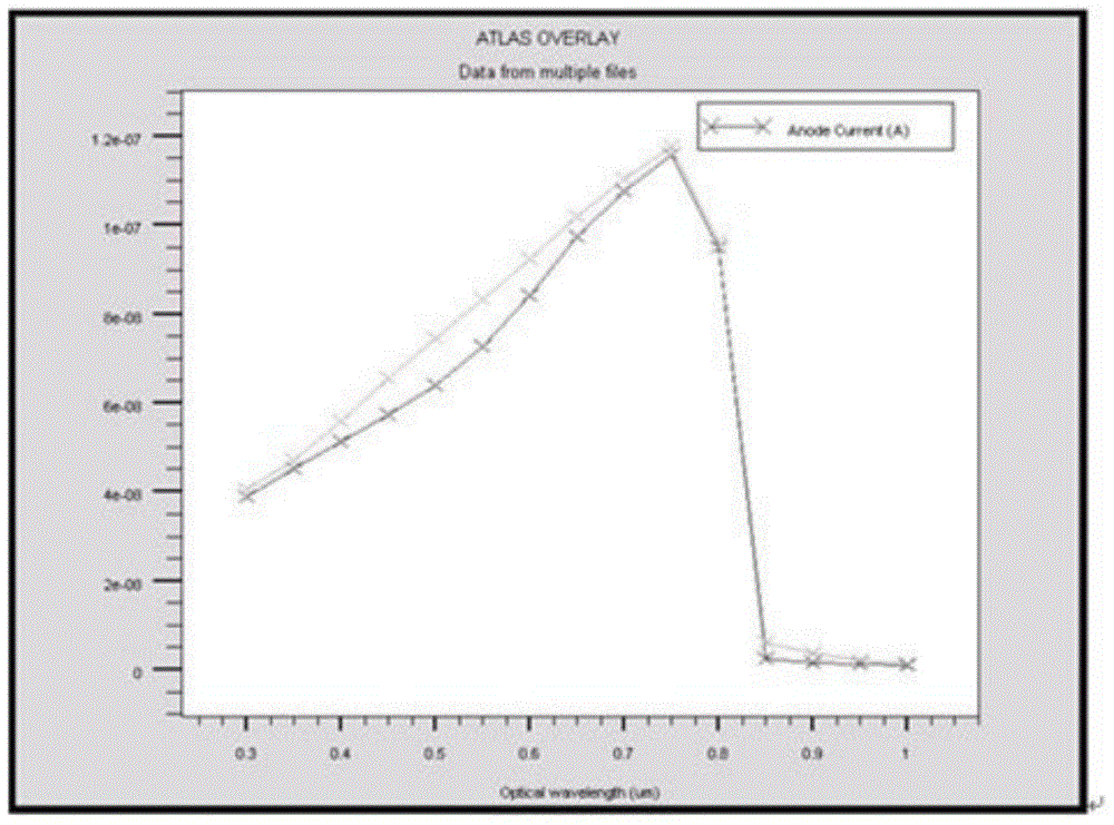
[0022] Embodiment 1, battery spectral response simulation test.

[0023] The results of this test can be found in image 3 ,from image 3 It can be seen that the change trend of the spectral response of the two batteries is the same, both increase with the increase of the wavelength in the 300-850nm band, and the spectral response intensity decreases rapidly after 850nm. From the change trend of spectral response, the main part of solar energy absorbed by the solar cell of the present invention is still in the polycrystalline silicon substrate. The spectral response peak at 850nm is related to the forbidden band width of polysilicon, that is, this wavelength is equivalent to the forbidden band width of polysilicon.

[0024] The response intensity of the battery in the invention is stronger than that of the single-junction polycrystalline silicon solar battery in the whole spectral region, especially in the 400-600nm band and the band after 850nm. It can be seen from the in...

Embodiment 2

[0025] Embodiment 2, open circuit voltage simulation experiment.

[0026] The results of this test can be found in Figure 5 , in the 300-850nm band, the open circuit voltage of the battery of the present invention is basically the same as that of the single-junction polycrystalline silicon battery, and both increase with the increase of the wavelength. But in the 850nm band, the voltage of the battery of the present invention is greatly improved compared with the single-junction polycrystalline silicon battery. This is because from the battery structure, the electrodes of the two batteries are all deposited on polysilicon, so the open circuit voltage does not change much before 850nm, but the spectral response in the long-wave band is stronger than that of the single-junction polysilicon battery, so the present invention The voltage of the battery in the long-wave band is stronger than that of the single-junction polycrystalline silicon battery.

Embodiment 3

[0027] Example 3, the effect of α-si film thickness on the spectral response of the battery The results of this test can be found in Image 6 , Image 6 Shown in the α-si thin film thickness of 0.01, 0.1, 0.5, 1μm and the spectral response of polycrystalline silicon cells. It can be seen from the figure that as the thickness of the α-si (amorphous silicon) film increases, the spectral response intensity in the 300-850nm band gradually decreases, and after the wavelength of 850nm, the spectral response gradually increases with the increase of the film thickness. This shows that as the thickness increases, the incident light of shorter wavelength is absorbed by the film itself, resulting in a decrease in the light intensity reaching the substrate, and the spectral response decreases with the increase of film thickness. However, since the long wave cannot be absorbed by the film with a wide band gap, the absorption of the long wave by the polysilicon substrate increases, so tha...


PUM

PropertyMeasurementUnit
thicknessaaaaaaaaaa

Abstract

The invention relates to a preparation method of a silica-based laminated solar cell. The preparation method comprises steps as follows: step one, a PN-junction cell is prepared by utilizing a polycrystalline silicon substrate; step two, an aluminum top electrode is deposited and is in ohmic contact with P-type polycrystalline silicon; step three, a P-type polycrystalline silicon layer is deposited and forms homotype heterojunction with the P-type polycrystalline silicon; step four, a bottom electrode is prepared, and the laminated solar cell is formed. According to the preparation method of the silica-based laminated solar cell, an amorphous silicon membrane of a top wide-band gap is taken as a light absorption layer to form the heterojunction with the polycrystalline silicon substrate, polycrystalline silicon of a bottom wide-band gap is taken as a light absorption layer, PN junctions are formed in the polycrystalline silicon, and the two junctions share one P-type polycrystalline silicon layer, so that one inter-cell interface is reduced, the combined action of the inter-cell interfaces on electric current is avoided, and the photoelectric conversion efficiency of the solar cell is increased by 5%-10% compared with a single-junction polycrystalline silicon cell.

Description

technical field [0001] The invention relates to solar cell technology, in particular to a method for preparing a silicon-based stacked solar cell. Background technique [0002] A solar cell is a photoelectric energy conversion device that can convert light energy into electrical energy without any pollutant emissions during the conversion process. It is one of the most important clean energy sources. The basic principle is to use the PN junction composed of semiconductor materials, and light to generate electron-hole pairs in the solar cell, through the electric field of the PN junction, and lead out through the electrodes to form a photocurrent. Since sunlight is composed of light waves of different wavelengths, and solar cells can only absorb photons whose energy is greater than its energy gap value, only a part of the energy in sunlight is converted into electrical energy, and most of it is absorbed by electrodes and semiconductor materials and becomes useless. heat ener...

Claims


Application Information

Patent Timeline
Patent Type & Authority Applications(China)
IPC IPC(8): H01L31/18
CPCY02P70/50
Inventor 王强
Owner NANTONG UNIVERSITY
Features
  • R&D
  • Intellectual Property
  • Life Sciences
  • Materials
  • Tech Scout
  • Unparalleled Data Quality
  • Higher Quality Content
  • 60% Fewer Hallucinations
Learn More