Group III semiconductor luminescent device

A technology of light-emitting devices and semiconductors, which is applied in the direction of semiconductor devices, electrical components, circuits, etc., can solve the problem of excessive etching of the active layer, achieve the effect of increasing the light-emitting area and improving the photoelectric characteristics

Inactive Publication Date: 2015-05-27
XIANGNENG HUALEI OPTOELECTRONICS
View PDF2 Cites 10 Cited by
  • Summary
  • Abstract
  • Description
  • Claims
  • Application Information

AI Technical Summary

Problems solved by technology

[0006] In order to solve the problems in the above-mentioned prior art, the object of the present invention is to provide a III-group semiconductor light-emitting device to solve the problem of excessive etch

Method used


Image

  • Group III semiconductor luminescent device
  • Group III semiconductor luminescent device
  • Group III semiconductor luminescent device

Examples


Embodiment 1

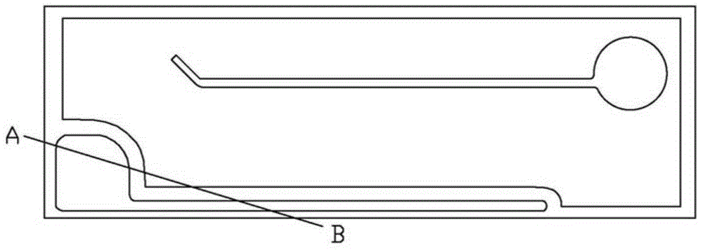
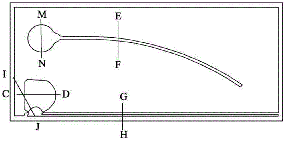
[0085] like image 3 As shown, it is a top view of the Group III semiconductor light-emitting device provided in this embodiment, Figure 4a-Figure 4c for image 3 The cross-sectional view of the N-type pad in the I-J direction to the N-type line electrode; Figure 5a to Figure 5d for image 3 The cross-sectional view of the P-type pad in the M-N direction; Figure 6a and Figure 6b for image 3 The cross-sectional view of the N-type pad in the C-D direction; Figure 7a-7d for image 3 The cross-sectional view of the P-type wire electrode in the E-F direction; Figures 8a-8d for image 3 The cross-sectional view of the N-type wire electrode in the G-H direction; Figure 9 is a top view of the N-type wire electrode and the active layer below it; Figure 10 for Figure 9 A cross-sectional view of the active layer under the N-type line electrode being reduced; Figure 11a and Figure 11b It is a wire bonding pad-insulating layer-transparent conductive layer and its e...

Embodiment 2

[0108] On the basis of embodiment 1, image 3 is a top view of the Group III semiconductor light-emitting device provided in this embodiment, and Figure 4a to ~ Figure 8d respectively image 3 cross-sectional view.

[0109] Figure 5a-5d , Figure 6a , Figure 6b respectively image 3 The cross-sectional view of the P-type pad 11 and the N-type pad 12 along the M-N and C-D section lines, it can be seen that the P-type pad 11 and the N-type pad 12 are all located above the active layer 4, wherein Figure 5a , Figure 5b , Figure 6a , Figure 6b The structure can be located anywhere above the insulating layer, and it is easier to design the mask pattern because it does not affect the current distribution.

[0110] Figure 5a , Figure 5b , Figure 6a and Figure 6b The bottom of the P-type pad 11 and N-type pad 12 is an insulating layer, so it does not participate in the current distribution. Therefore, only the P-type wire electrode 13 and the N-type wire elect...

Embodiment 3

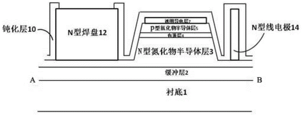
[0114] like Figure 12 As shown, the Group III nitride semiconductor light-emitting device provided in this embodiment includes a substrate 1, a buffer layer 2, an n-type nitride semiconductor layer 3, an active layer 4, and a p-type nitride semiconductor layer arranged sequentially from bottom to top. layer 5, transparent conductive layer 7 and insulating layer 15.

[0115] The five layers of the substrate 1 , the buffer layer 2 , the n-type nitride semiconductor layer 3 , the active layer 4 and the p-type nitride semiconductor layer 5 constitute the structure of the boss 16 .

[0116] The upper surface of the boss 16 is the upper surface of the p-type nitride semiconductor layer.

[0117] An N-type wire electrode 14 is provided on the boss, and the N-type wire electrode 14 is in contact with the n-type nitride semiconductor layer 3 .

[0118] The active layer 4 below the N-type line electrode 14 is partially etched away (see Figure 9 ).

[0119] The N-type wire electrod...


PUM

PropertyMeasurementUnit
Thicknessaaaaaaaaaa
Thicknessaaaaaaaaaa
Thicknessaaaaaaaaaa

Abstract

The invention discloses a group III semiconductor luminescent device. The luminescent device comprises a substrate, a buffer layer, an n-shaped nitride semiconductor layer, an active layer and a p-shaped nitride semiconductor layer which are arranged from bottom to top in sequence and form a boss, wherein the upper surface of the p-shaped nitride semiconductor layer serves as the upper surface of the boss; an N-shaped line electrode is further arranged on the surface of the boss; the active layer below the N-shaped line electrode is etched or partially etched; the N-shaped line electrode is further connected with an N-shaped bonding pad; the N-shaped bonding pad is positioned above the active layer; the N-shaped line electrode and the N-shaped bonding pad form an N-shaped electrode; the luminescent device further comprises a P-shaped electrode; the P-shaped electrode comprises a P-shaped bonding pad and a P-shaped line electrode; the P-shaped line electrode is positioned on the boss. The luminescent device solves the problem that the active layer is excessively etched, improves the electrical and optical properties through added the active layer, increases the luminescent area, and ensures that the operating voltage is reduced and the brightness is improved.

Description

technical field [0001] The present application relates to the technical field of semiconductor lighting, in particular to a III-group semiconductor light-emitting device. Background technique [0002] The luminous efficiency of gallium nitride-based light-emitting diodes has been greatly improved in recent years, but the external quantum efficiency and the uniformity of current distribution have become the main technical bottlenecks restricting the further improvement of the performance of light-emitting diodes. In the prior art, gallium nitride-based light-emitting diodes on sapphire substrates are located on the same substrate because of their P-type electrodes and N-type electrodes. The P-type electrodes and N-type electrodes generally include wire bonding pads and wire electrodes. The wire bonding pad of the N-type electrode is used to solder gold balls (the diameter of the gold ball is generally 75um), so the size of the N-type electrode wire bonding pad is designed to ...

Claims


Application Information

Patent Timeline
IPC IPC(8): H01L33/38H01L33/62H01L33/44
CPCH01L33/38H01L33/385H01L33/62
Inventor 许顺成
Owner XIANGNENG HUALEI OPTOELECTRONICS
Why Eureka
Try Eureka