Organic electroluminescence device and preparation method thereof

An electroluminescent device and luminescence technology, which is applied in the direction of electric solid-state devices, semiconductor/solid-state device manufacturing, electrical components, etc., can solve problems such as poor refractive index, low light extraction performance, total reflection loss, etc., and achieve improved hole injection Efficiency, improvement of luminous efficiency, and the effect of improving conductivity

Inactive Publication Date: 2015-05-27
OCEANS KING LIGHTING SCI&TECH CO LTD +2
View PDF0 Cites 0 Cited by
  • Summary
  • Abstract
  • Description
  • Claims
  • Application Information

AI Technical Summary

Problems solved by technology

[0003] In traditional light-emitting devices, only about 18% of the light inside the device can be emitted to the outside, while the rest will be consumed outside the device in other forms, and there is a difference in refractive index between the interfaces (such as between glass and ITO). The difference between the refractive index, the refractive index of glass is 1.5, ITO is 1.8, the light from ITO reaches the glass, and total reflection will occur), which causes the loss of total reflection, resulting in lower overall light extraction performance

Method used


Image

  • Organic electroluminescence device and preparation method thereof
  • Organic electroluminescence device and preparation method thereof

Examples


preparation example Construction

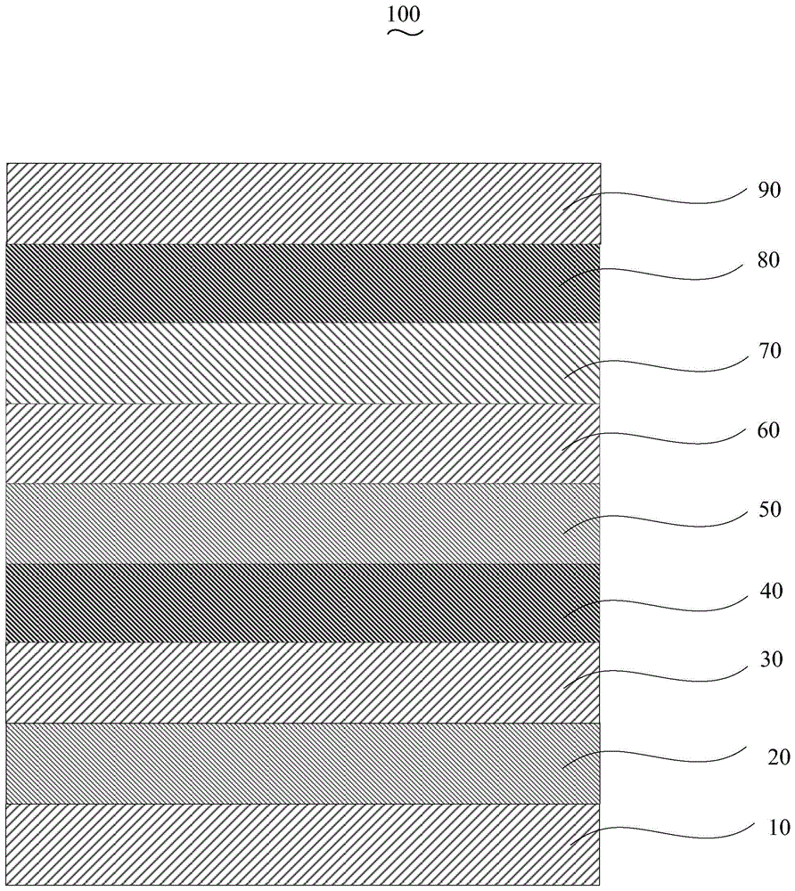
[0036] The preparation method of the organic electroluminescence device 100 of an embodiment, it comprises the following steps:

[0037] Step S110 , preparing the scattering layer 20 on the surface of the glass substrate 10 by electron beam evaporation.

[0038] The scattering layer 20 is formed on one side surface of the glass substrate 10 . The scattering layer 20 includes a metal material, a hole transport material and a luminescent material. The scattering layer 20 is prepared on the surface of the glass substrate 10 by thermal resistance evaporation. The work function of the metal material is -2.0eV~-3.5eV, and the The hole transport material is selected from 1,1-bis[4-[N,N'-bis(p-tolyl)amino]phenyl]cyclohexane (TAPC), 4,4',4''-tris( At least one of carbazol-9-yl)triphenylamine (TCTA), N,N'-(1-naphthyl)-N,N'-diphenyl-4,4'-biphenylenediamine (NPB) , the material of the luminescent material layer is selected from: 4-(dinitrile methyl)-2-butyl-6-(1,1,7,7-tetramethyljulones...

Embodiment 1

[0059] The structure prepared in this example is glass substrate / Mg:Alq 3 :TAPC / ITO / MoO 3 / NPB / Alq 3 / TAZ / CsF / Ag organic electroluminescent device, in this embodiment and the following embodiments, " / " indicates a layer, and ":" indicates doping.

[0060] The glass substrate is N-LASF44. After rinsing the glass substrate with distilled water and ethanol, soak it in isopropanol for one night. Prepare the scattering layer on the glass substrate, the scattering layer includes metal materials, hole transport materials and luminescent materials, and prepare the scattering layer on the surface of the glass substrate by thermal resistance evaporation, the material is Mg:Alq 3 : TAPC, Mg, Alq 3 The mass ratio to TAPC is 5:3:1, and the thickness is 300nm. Then ITO is prepared on the scattering layer with a thickness of 100nm, which is prepared by magnetron sputtering; the hole injection layer is prepared by evaporation: the material is MoO 3 , with a thickness of 40nm; the hole tr...

Embodiment 2

[0067] The structure prepared in this example is glass substrate / Sr:DCJTB:TCTA / IZO / V 2 o 5 / NPB / DCJTB / TPBi / Cs 2 CO 3 / Al organic electroluminescent devices.

[0068] The glass substrate is N-LAF36. After rinsing the glass substrate with distilled water and ethanol, soak it in isopropanol for one night to prepare a scattering layer on the glass substrate. The surface of the substrate is prepared by thermal resistance evaporation, and the material is Sr:DCJTB:TCTA, Sr, the mass ratio of DCJTB to TCTA is 1:0.5:1, and the thickness is 80nm. Then IZO is prepared on the scattering layer with a thickness of 80nm, prepared by magnetron sputtering; the hole injection layer is evaporated, and the material is V 2 o 5 , with a thickness of 40nm; evaporated hole transport layer: the material is NPB, with a thickness of 45nm; evaporated luminescent layer: the selected material is DCJTB, with a thickness of 8nm; evaporated electron transport layer, the material is TPBi, with a thickness...


PUM


Abstract

The invention discloses an organic electroluminescence device which comprises a glass substrate, a scattering layer, an anode, a hole injection layer, a hole transmission layer, a light emitting layer, an electron transfer layer, an electron injection layer and a cathode which are overlapped in sequence, wherein the scattering layer comprises a metal material, a hole transfer material and a light emitting material; the power function of the metal material is minus 2.0-minus 3.5eV; the hole transfer material is selected from at least one of 1,1-di[4-[N,N'-di(p-cresyl)amino]phenyl]cyclohexane, 4,4',4''-tri(carbazole-9-yl)triphenylamine and N,N'-(1-naphthyl)-N,N'-diphenyl-4,4'-benzidine. The organic electroluminescence device disclosed by the invention is relatively high in light emission efficiency. The invention further provides a preparation method of the organic electroluminescence device.

Description

technical field [0001] The invention relates to an organic electroluminescence device and a preparation method thereof. Background technique [0002] The luminescence principle of organic electroluminescent devices is based on the action of an external electric field, electrons are injected from the cathode to the lowest unoccupied molecular orbital (LUMO) of organic matter, and holes are injected from the anode to the highest occupied molecular orbital (HOMO) of organic matter. Electrons and holes meet, recombine, and form excitons in the light-emitting layer. Excitons migrate under the action of an electric field, transfer energy to the light-emitting material, and excite electrons to transition from the ground state to the excited state. The excited state energy is deactivated by radiation to generate photons , releasing light energy. [0003] In traditional light-emitting devices, only about 18% of the light inside the device can be emitted to the outside, while the res...

Claims


Application Information

Patent Timeline
Patent Type & Authority Applications(China)
IPC IPC(8): H01L51/50H01L51/52H01L51/54H01L51/56
CPCH10K50/00H10K50/854H10K71/00
Inventor 周明杰黄辉陈吉星王平
Owner OCEANS KING LIGHTING SCI&TECH CO LTD
Why Eureka
Try Eureka