Forming method of semiconductor device and grid electrode

A semiconductor and device technology, applied in the field of semiconductor preparation, can solve the problems affecting the etching process of the polysilicon layer 11 of the hard mask layer, the flatness of the sidewall of the photoresist pattern, and affecting the structure of the polysilicon gate, etc., to ensure accurate degree, reduce surface roughness, optimize the effect of photoresist pattern structure

Active Publication Date: 2015-06-03
SEMICON MFG INT (SHANGHAI) CORP
View PDF5 Cites 4 Cited by
  • Summary
  • Abstract
  • Description
  • Claims
  • Application Information

AI Technical Summary

Problems solved by technology

However continue to refer to figure 1 As shown, after the exposure process, the flatness of the sidewall of the formed photoresist pattern is poor, which affects the subsequent etching process of the hard mask layer 12 and the polysilicon layer 11, and finally affects the formed polysilicon gate. The structure, such as the line width roughness (Line Width Roughness) of the polysilicon gate is relatively large, thereby reducing the performance of the final polysilicon gate

Method used


Image

  • Forming method of semiconductor device and grid electrode
  • Forming method of semiconductor device and grid electrode
  • Forming method of semiconductor device and grid electrode

Examples


Embodiment Construction

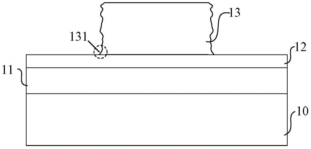
[0040] As mentioned in the background art, with the increase of the integration level of integrated circuits, the device size of integrated circuits decreases continuously, and the quality requirements for devices become more and more stringent. However, in the existing photolithography technology, the flatness of the sidewall of the photoresist pattern formed after the photoresist exposure and development process is poor, which in turn will affect the subsequent use of the photoresist pattern as a mask such as a hard mask. The etching precision of the layer affects the quality of the integrated circuit device formed by subsequent etching processes.

[0041] For this reason, after the photoresist pattern is formed, the industry will use HBr and other gases to cure the soft photoresist pattern (HBr cure), and form a polymer modification layer on the surface of the photoresist pattern to improve The flatness of the photoresist pattern surface such as sidewalls.

[0042] However...


PUM


Abstract

The invention provides a forming method of a semiconductor device and a grid electrode. In the forming method of the semiconductor device, a photoresist layer arranged above a hard mask layer is subjected to patterning, and after photoresist patterns are formed, the photoresist patterns are subjected to softening processing process, so that the surface roughness degree of the photoresist patterns is effectively reduced, then, the photoresist patterns are used as marks for etching the partial hard mask layer, the remained photoresist at the bottom of the side wall of the photoresist patterns is removed, then, the photoresist patterns are subjected to tightening processing process, the photoresist patterns are cured, meanwhile, a decoration layer is formed on the surfaces of the photoresist patterns, the smoothness of the side wall surface of the photoresist patterns is improved, the quality of the hard mask patterns subsequently obtained by using the photoresist patterns as the marks for etching the hard mask layer can be improved, and further, the structure precision of the semiconductor device obtained after the hard mask patterns are used as the masks for etching the materials to be etched in the subsequent steps can be improved, so that the performance of the semiconductor device is optimized.

Description

technical field [0001] The invention relates to the field of semiconductor preparation, in particular to a method for forming a semiconductor device and a gate. Background technique [0002] With the development of integrated circuit manufacturing technology, the integration degree of integrated circuits is increasing, and the feature size of integrated circuits is also decreasing. Therefore, the quality requirements for electrical components in integrated circuits are becoming more and more stringent. [0003] In the integrated circuit manufacturing process, the photolithography process is considered to be the core step in the large-scale integrated circuit manufacturing process. The photolithography process is a process of transferring the pattern on the mask plate to each thin film layer of the semiconductor substrate through exposure, and then etching each thin film layer to form a thin film layer with a specific pattern. [0004] The development of modern photolithogra...

Claims


Application Information

Patent Timeline
Patent Type & Authority Applications(China)
IPC IPC(8): H01L21/027H01L21/28
Inventor 隋运奇
Owner SEMICON MFG INT (SHANGHAI) CORP
Why Eureka
Try Eureka