Inductive coil group and inductive coupling plasma processing device

An inductive coil and plasma technology, applied in the direction of plasma and electrical components, can solve the problems of waste of radio frequency energy, the inability of the plasma to be ignited reliably, and the reduction of the efficiency of electric energy use.

Active Publication Date: 2015-06-03
ADVANCED MICRO FAB EQUIP INC CHINA
View PDF7 Cites 12 Cited by
  • Summary
  • Abstract
  • Description
  • Claims
  • Application Information

AI Technical Summary

Problems solved by technology

[0004] However, such a reaction chamber structure will also bring serious problems: due to the existence of the Faraday shielding plate, the electric field generated on the induction coil cannot enter the reaction chamber, and only part of the magnetic field can enter, which will cause the plasma to be unable to be reliably ignited when the plasma is ignited. Additional devices or higher power input RF coils are required to ensure plasma ignition
The impedance of the plasma will change sharply before and after ignition, from a high-impedance substance to a conductor in an instant, and the matching device that adjusts the input RF power needs a mechanical structure to adjust the impedance matchin

Method used


Image

  • Inductive coil group and inductive coupling plasma processing device
  • Inductive coil group and inductive coupling plasma processing device
  • Inductive coil group and inductive coupling plasma processing device

Examples


Embodiment Construction

[0039] In order to make the content of the present invention clearer and easier to understand, the content of the present invention will be further described below in conjunction with the accompanying drawings. Of course, the present invention is not limited to this specific embodiment, and general replacements known to those skilled in the art are also covered within the protection scope of the present invention.

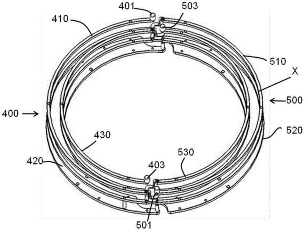
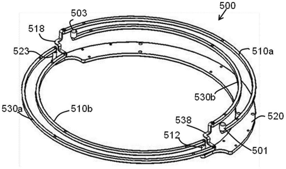
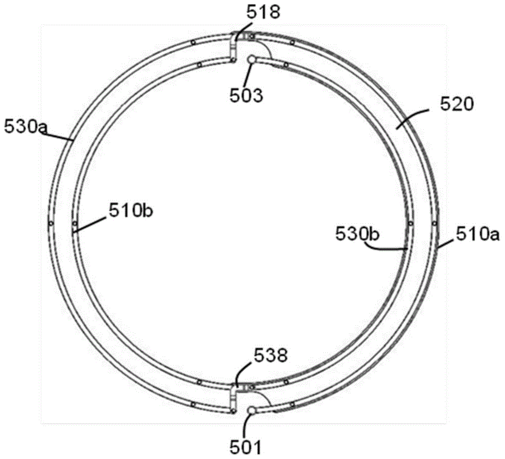
[0040] figure 1 ~ Fig. 2 has shown the embodiment of the inductance coil of the present invention. It should be understood that the plasma processing device in the present invention can be a device such as plasma etching, plasma physical vapor deposition, plasma chemical vapor deposition, plasma surface cleaning, etc., and the plasma processing device is only exemplary. Fewer or more constituent elements may be included, or the arrangement of the constituent elements may be the same as or different from that shown in the drawings.

[0041] See figure 1 , which i...


PUM


Abstract

The invention discloses a plasma processing device. The plasma processing device comprises an air-tight reaction chamber, wherein the reaction chamber comprises a reaction chamber sidewall and a top insulating material window, and the reaction chamber therein comprises a base for supporting a substrate to be processed; a self-shielding inductive coil group is fixedly arranged above the insulating material window. The plasma processing device is characterized in that the self-shielding inductive coil group comprises a plurality of inductive coils, each inductive coil comprises a flat-plate-shaped intermediate coil, a plurality of intermediate coils are combined to form a shielding ring, the two ends of each intermediate coil respectively comprise an input coil and an output coil, wherein the input coil and the output coil are spirally upward from the two ends of the intermediate coil and are respectively connected to a radio-frequency power supply and a regulating circuit, and downward projections of the input coil and the output coil are located on at least one intermediate coil. By adopting the inductive coil structure disclosed by the invention, the capacity coupling of the inductive coil towards the inside of the reaction chamber can be reduced and the service life of the insulating material window can be improved.

Description

technical field [0001] The invention relates to plasma processing equipment, in particular to an inductive coupling coil of a plasma processing device. Background technique [0002] In recent years, with the development of semiconductor manufacturing processes, the requirements for the integration and performance of components are getting higher and higher, and plasma technology (Plasma Technology) has been widely used. Plasma technology introduces a reactive gas and electron flow into the reaction chamber of the plasma processing device, uses a radio frequency electric field to accelerate the electrons, and collides with the reactive gas to ionize the reactive gas and generate plasma. The generated plasma can be used Used in various semiconductor manufacturing processes, such as deposition processes (such as chemical vapor deposition), etching processes (such as dry etching), etc. [0003] Plasma processing equipment includes common capacitively coupled and inductively cou...

Claims


Application Information

Patent Timeline
IPC IPC(8): H05H1/46
Inventor 王俊倪图强左涛涛
Owner ADVANCED MICRO FAB EQUIP INC CHINA
Why Eureka
Try Eureka