Preparation method and structure of fully intermetallic compound interconnection solder joints
An intermetallic compound and compound technology, which is used in metal processing equipment, metal processing, welding equipment, etc., can solve the problems of different orientations of intermetallic compounds, influence on the reliability of micro-solder joints, and easy generation of micro-voids, etc. Efficiency, suitable for large-scale production, the effect of avoiding high temperature damage
- Summary
- Abstract
- Description
- Claims
- Application Information
AI Technical Summary
Problems solved by technology
Method used
Image

Examples
Embodiment 1
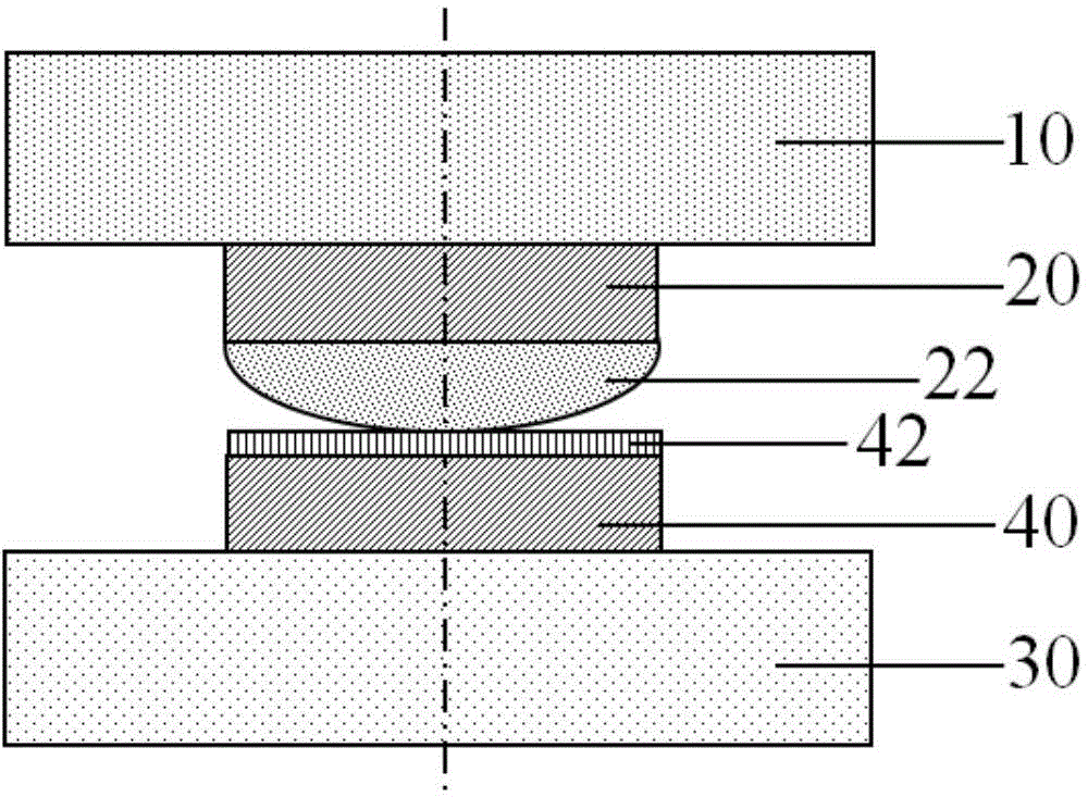
[0040] Such as figure 1 , figure 2 and Figure 5 As shown, the preparation method of the all-intermetallic compound interconnect solder joint of the present invention can be realized through the following specific process steps:
[0041] Step 1: Provide a first substrate 10, sputter an array of single crystal Cu first metal pads 20 with a thickness of 1 μm on the first substrate 10, and anneal the single crystal Cu first metal pads 20 on the first substrate 10. Sn is electroplated on the top, and Sn solder bumps 22 with a diameter of 1 μm are formed after reflow; a second substrate 30 is provided, and an array of polycrystalline Cu second metal pads 40 with a thickness of 2 μm is sputtered on the second substrate 30, Make the single crystal Cu first metal pad 20 and the polycrystalline Cu second metal pad 40 have the same array pattern, and electroplate a Ni / Au solderable layer 42 on the polycrystalline Cu second metal pad 40;
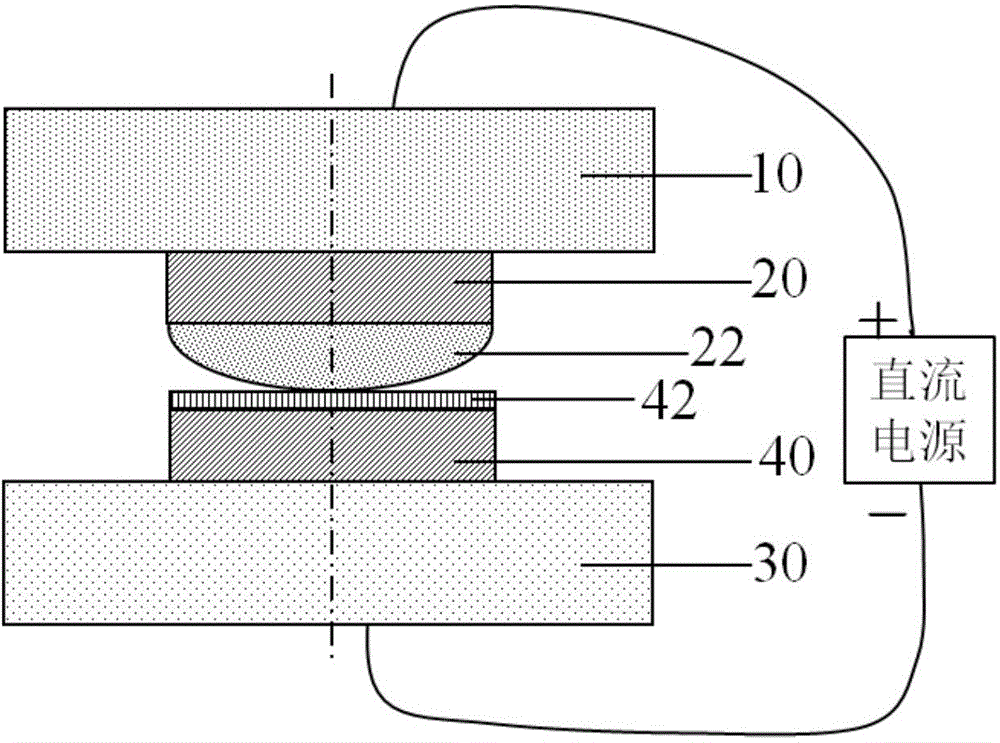
[0042] Step 2: aligning the Sn solder bump 2...
Embodiment 2
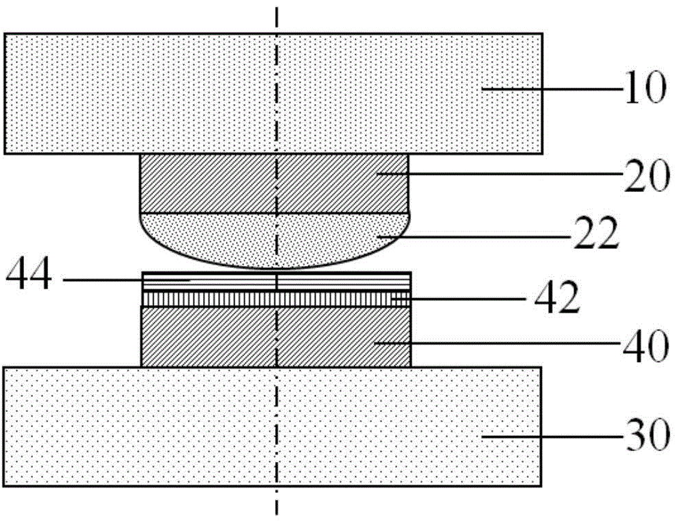
[0046] Such as image 3 , Figure 4 and Figure 5 As shown, the preparation method of the all-intermetallic compound interconnect solder joint of the present invention can be realized through the following specific process steps:
[0047] Step 1: Provide a first substrate 10, plate an array of Ni first metal pads 20 with a thickness of 5 μm and a good preferred orientation on the first substrate 10, and perform annealing treatment on the Ni first metal pads 20 with a preferred orientation. Sn is electroplated on it, and Sn solder bumps 22 with a diameter of 10 μm are formed after reflow; a second substrate 30 is provided, and an array of polycrystalline Ni second metal pads 40 with a thickness of 20 μm is electroplated on the second substrate 30, Make the array pattern of the preferred orientation Ni first metal pad 20 and the polycrystalline Ni second metal pad 40 the same, and electroplate the Au solderable layer 42 on the polycrystalline Ni second metal pad 40;
[0048] ...
Embodiment 3
[0051] Such as figure 1 , figure 2 and Figure 5 As shown, the preparation method of the all-intermetallic compound interconnect solder joint of the present invention can be realized through the following specific process steps:
[0052] Step 1: Provide a first substrate 10, plate an array of Cu first metal pads 20 with a thickness of 30 μm on the first substrate 10 and have a good preferred orientation, and anneal the Cu first metal pads 20 with a preferred orientation. Sn is electroplated on it, and Sn solder bumps 22 with a diameter of 100 μm are formed after reflow; a second substrate 30 is provided, and an array of polycrystalline Cu second metal pads 40 with a thickness of 100 μm is electroplated on the second substrate 30, Make the array patterns of the preferred orientation Cu first metal pad 20 and the polycrystalline Cu second metal pad 40 the same, and chemically deposit an OSP solderable layer 42 on the polycrystalline Cu second metal pad 40;
[0053] Step 2: a...
PUM
| Property | Measurement | Unit |
|---|---|---|
| current density | aaaaa | aaaaa |
| diameter | aaaaa | aaaaa |
| diameter | aaaaa | aaaaa |
Abstract
Description
Claims
Application Information
 - R&D
- Intellectual Property
- Life Sciences
- Materials
- Tech Scout
- Unparalleled Data Quality
- Higher Quality Content
- 60% Fewer Hallucinations
Browse by: Latest US Patents, China's latest patents, Technical Efficacy Thesaurus, Application Domain, Technology Topic, Popular Technical Reports.
© 2025 PatSnap. All rights reserved.Legal|Privacy policy|Modern Slavery Act Transparency Statement|Sitemap|About US| Contact US: help@patsnap.com