LDMOS transistor and forming method thereof

A transistor and body region technology, applied in semiconductor devices, semiconductor/solid-state device manufacturing, electrical components, etc., can solve the problems of fringe electric field enhancement of device size, unsuitable device size reduction, increased on-resistance, etc., to improve current, Effect of electric field reduction and on-resistance reduction

Inactive Publication Date: 2015-06-10
SEMICON MFG INT (SHANGHAI) CORP
View PDF3 Cites 1 Cited by
  • Summary
  • Abstract
  • Description
  • Claims
  • Application Information

AI Technical Summary

Problems solved by technology

[0005] However, increasing the lateral distance FX of the isolation structure 31 brings adverse effects in three aspects at the same time: 1. The on-resistance increases; 2. The electric field at the edge of the gate 42 and the isolation structure 31 increases, which increases the risk of breakdown; 3. No Suitable for today's device size reduction trend
[0006] For this reason, a new LDMOS transistor and its formation method are needed to prevent the problems of increased on-resistance, enhanced fringe electric field and increased device size when the breakdown voltage is increased

Method used


Image

  • LDMOS transistor and forming method thereof
  • LDMOS transistor and forming method thereof
  • LDMOS transistor and forming method thereof

Examples


Embodiment Construction

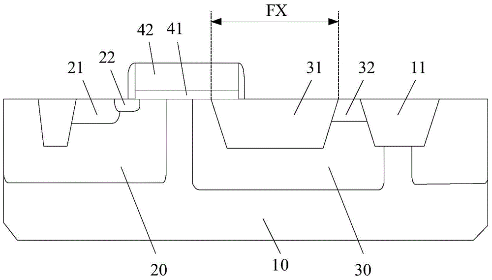
[0041] Existing LDMOS transistors achieve the purpose of increasing the breakdown voltage by extending the isolation structure in the drift region, but this approach brings various adverse effects, such as the on-resistance increases with the increase of the length of the isolation structure, the gate and the isolation structure The electric field at the edge also increases with the length of the isolation structure, and the size of the overall device structure increases accordingly.

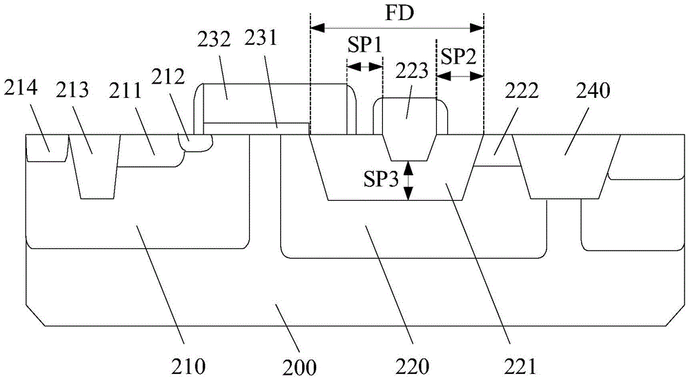
[0042] To this end, the present invention provides a novel LDMOS transistor, the LDMOS transistor has a gate region on the semiconductor substrate, a body region and a drift region in the semiconductor substrate on both sides of the gate region, located A source region in the body region, a drain region in the drift region, a first isolation structure in the drift region and between the gate region and the drain region, and a first isolation structure in the drift region The control electrode on...


PUM


Abstract

Disclosed are an LDMOS transistor and a forming method thereof. The LDMOS transistor comprises a transistor body region and a shifting region which are located on a semiconductor substrate, a gate region, a source region located in the transistor body region, a leakage region located in the shifting region, a first isolation structure and a control electrode; a clearance is formed between the transistor body region and the shifting region; the gate region spans above the transistor body region and the shifting region; the source region and the leakage region are located on two sides of the gate region; the first isolation structure is located in the shifting region and between the gate region and the leakage region; the control electrode is located on the first isolation structure, and the bottom of the control electrode is located in the first isolation structure. The LDMOS transistor has the advantages that the size increase is avoided, the breakdown voltage is increased, and the conduction resistance is decreased.

Description

technical field [0001] The invention relates to the field of semiconductor manufacturing, in particular to an LDMOS transistor and a forming method thereof. Background technique [0002] Laterally Diffused Metal Oxide Semiconductor (LDMOS) transistors are mainly used in power integrated circuits, such as RF power amplifiers for mobile phone base stations, and can also be used in high frequency (HF), very high frequency (VHF) and Ultra-high frequency (UHF) broadcast transmitters and microwave radar and navigation systems, etc. LDMOS technology brings higher power peak-to-average ratio, higher gain and linearity to the new generation of base station amplifiers, and at the same time brings higher data transmission rates to multimedia services. [0003] For an LDMOS transistor used as a power integrated circuit, its on-resistance (Rdson) and breakdown voltage (Breakdown Voltage, BV) are two important indicators to measure its device performance. For LDMOS, it is usually expect...

Claims


Application Information

Patent Timeline
Patent Type & Authority Applications(China)
IPC IPC(8): H01L29/78H01L29/10H01L21/336
Inventor 曹国豪郑大燮
Owner SEMICON MFG INT (SHANGHAI) CORP
Why Eureka
Try Eureka