Large-area graphene preparing method based on high-density ordered copper nanowire catalyst

A copper nanowire, high-density technology, applied in the field of microelectronics, can solve the problem of difficulty in preparing large-area graphene, and achieve the effect of uniform pore size and uniform distribution

Active Publication Date: 2015-06-24
XIDIAN UNIV
View PDF5 Cites 6 Cited by
  • Summary
  • Abstract
  • Description
  • Claims
  • Application Information

AI Technical Summary

Problems solved by technology

[0006] The purpose of the present invention is to provide a large-area graphene preparation method based on high-density ordered copper nanowire catalysis, to solve the problem that it is difficult to prepare large-area graphene using copper foil

Method used


Image

  • Large-area graphene preparing method based on high-density ordered copper nanowire catalyst
  • Large-area graphene preparing method based on high-density ordered copper nanowire catalyst
  • Large-area graphene preparing method based on high-density ordered copper nanowire catalyst

Examples


Embodiment 1

[0030] Embodiment 1: Making graphene catalyzed based on copper nanowires with a length of 10 um.

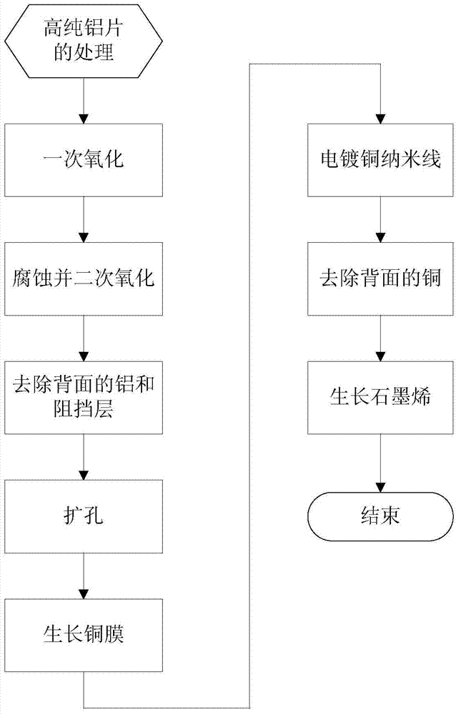
[0031] Step 1: Pre-treat the aluminum sheet.

[0032] (1a) Put the aluminum sheet with 99.999% purity into acetone, water and isopropanol solution successively, and ultrasonically remove the grease on the surface for 5 minutes each;

[0033] (1b) Put the ultrasonically finished aluminum sheet into a mixed acid solution and soak it at 60°C for 30 seconds to remove surface impurities. 1mL, water 69mL;

[0034] (1c) Put the aluminum sheet from which surface impurities have been removed into the polishing solution, and polish it at 20V for 4 minutes in constant voltage mode to make the aluminum sheet smooth. The polishing solution is composed of 25mL perchloric acid stock solution and 75mL anhydrous mixed with ethanol.

[0035] Step 2: Oxidize the pretreated aluminum sheet using constant voltage direct current mode.

[0036] (2a) Put the polished aluminum sheet into an oxalic aci...

Embodiment 2

[0051] Embodiment 2: Making graphene catalyzed based on copper nanowires with a length of 15 um.

[0052] The first step: pretreatment of aluminum sheet.

[0053] (A1) Put the aluminum flakes with 99.999% purity into acetone, water and isopropanol solutions and ultrasonically remove the grease on the surface for 7 minutes each;

[0054] (A2) Put the ultrasonically finished aluminum sheet into a mixed acid solution and soak it at 60°C for 32 seconds to remove surface impurities. 1mL, water 69mL;

[0055] (A3) Put the aluminum sheet that has removed surface impurities into the polishing solution, and polish it at 20V for 4 minutes and 30 seconds in constant voltage mode to make the aluminum sheet smooth. The polishing solution is composed of 25mL perchloric acid stock solution and 75mL mixed with ethanol.

[0056] Step 2: Oxidize the pretreated aluminum sheet using constant voltage direct current mode.

[0057] (B1) primary oxidation, put the polished aluminum sheet into an ...

Embodiment 3

[0072] Embodiment 3: Making graphene catalyzed based on copper nanowires with a length of 20 um.

[0073] Step 1, pretreating the aluminum sheet.

[0074] First put the 99.999% pure aluminum sheet into acetone, water and isopropanol solutions for 10 minutes to remove the surface grease; then put the aluminum sheet after ultrasonication into the mixed acid solution and soak it at 60°C The impurities on the surface are removed in 35 seconds. The ratio of the mixed acid solution is: 20mL of concentrated hydrochloric acid, 10mL of concentrated nitric acid, 1mL of hydrofluoric acid, and 69mL of water. Polish at 20V for 5 minutes to make the aluminum sheet flat. The polishing solution is mixed with 25mL of perchloric acid stock solution and 75mL of absolute ethanol.

[0075] Step 2: Oxidize the pretreated aluminum sheet by constant voltage direct current mode.

[0076] Put the polished aluminum sheet into the oxalic acid solution with a concentration of 0.5mol / L, and soak it for 2...


PUM


Abstract

The invention discloses a large-area graphene preparing method based on a high-density ordered copper nanowire catalyst, mainly aiming at solving the problem that graphene cannot be prepared from a copper foil in a large area at present. The preparing method comprises the following implementing steps: preparing a through-hole anodic aluminum oxide template by virtue of a method of secondary oxidation; depositing a layer of copper film on one surface of the through-hole anodic aluminum oxide template, using the copper film as an electrode, and preparing a high-density ordered copper nanowire in required size in the through-hole anodic aluminum oxide template; and finally catalyzing by taking the high-density ordered copper nanowire as a catalyst so as to promote the growth of graphene in a large area. Compared with graphene growing from existing copper foil catalyst, the graphene disclosed by the invention has the advantages of larger area and better quality, and the graphene is applicable to the manufacturing of semiconductor devices.

Description

technical field [0001] The invention belongs to the technical field of microelectronics, in particular to a preparation method of graphene, which can be used in the preparation of semiconductor devices. technical background [0002] With the development of integrated circuits, the critical dimensions of silicon-based devices have reached the theoretical and technical limits, and quantum effects have become the main mechanism. Traditional silicon-based devices based on diffusion-drift theory are limited by both physics and technology, and cannot continue to undertake The important task of Moore's Law, therefore, it is necessary to find a new generation of basic semiconductor materials and develop new theories and device models to meet the needs of the continued development of integrated circuits. [0003] Graphene material is a carbon-based two-dimensional crystal. It is the lightest and thinnest material known so far. The single layer is only atomically thick. It has extreme...

Claims


Application Information

Patent Timeline
Patent Type & Authority Applications(China)
IPC IPC(8): C23C16/26C23C16/02C25D11/12
Inventor 陆小力张吉文王东张进成郝跃
Owner XIDIAN UNIV
Why Eureka
Try Eureka