Device and method for measuring film thickness

A film thickness and measuring device technology, applied in the direction of measuring devices, optical devices, instruments, etc., can solve the problems of high price of microscopic instruments, change of coating rate, non-linear law, etc., and achieve easy popularization and application and simple operation. , the effect of low environmental requirements

Active Publication Date: 2017-09-05
WANXIN OPTICAL GRP +1
View PDF7 Cites 0 Cited by
  • Summary
  • Abstract
  • Description
  • Claims
  • Application Information

AI Technical Summary

Problems solved by technology

[0004] For the measurement of micro-nano opaque films, there are mainly two types of existing technologies: (1) The film thickness is calculated according to the empirical law that the coating thickness increases linearly with the coating time, but the detection results are not reliable, because the conditions of each coating cannot be completely Similarly, the rate of coating will change, thereby not conforming to the linear rule; (2) adopt high-precision microscopic equipment, such as atomic force microscope, transmission electron microscope, etc., the price of microscopic equipment is expensive, and the operation is complicated, which is not conducive to popularization, and it is harmful to thin film There are also special requirements for the performance of the nanometer film. For example, the scanning probe microscopic technology of the atomic force microscope requires the nano film to be tested to have sharp edges; industrial production urgently needs to develop a high-precision measuring device and method for the thickness of the micro-nano film. Low cost, no expensive equipment, easy to operate and popularize

Method used


Image

  • Device and method for measuring film thickness
  • Device and method for measuring film thickness
  • Device and method for measuring film thickness

Examples


Embodiment 1

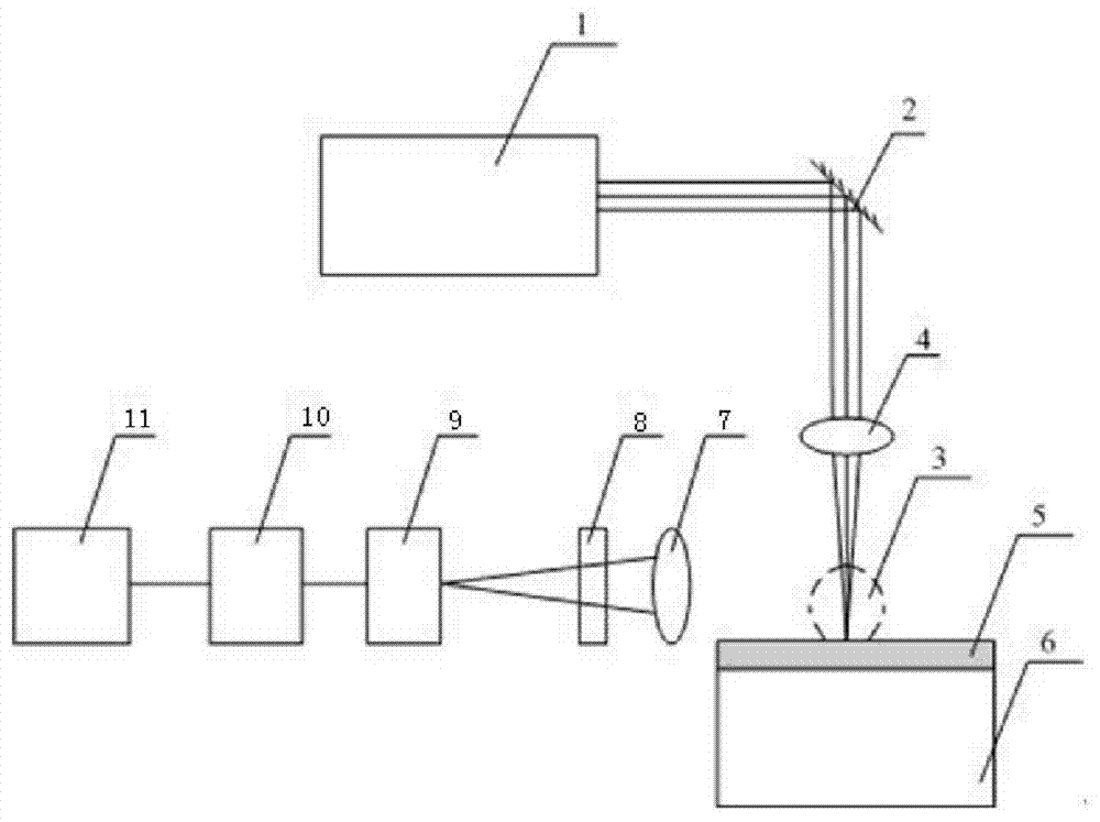
[0038] (1) Select laser 1 as SGR-10 series high-power pulsed Nd: YAG laser (SpitLight1000), output 1064nm infrared pulse Gaussian laser beam, laser pulse width 10ns, repetition frequency 10Hz, divergence angle ≤0.7mrad, single pulse laser The output energy is adjustable (the stable energy range is 50mJ~800mJ).

[0039] The photodetector 9 is selected as the photodiode of thorlab company, the model is DET10A / M, the rise time is less than 1ns, the response wavelength range is 200~1100nm, and the four-channel Yokogawa DL9140 oscilloscope is selected, the bandwidth is 1GHz, and the highest sampling rate is 2.5GS / s.

[0040] The focal length of the first focusing lens 4 is 160 mm, and the converging spot diameter is 50 um; the focal length of the second focusing lens 7 is 22.5 cm, and the plasma flash signal is converged on the receiving surface of the photodetector;

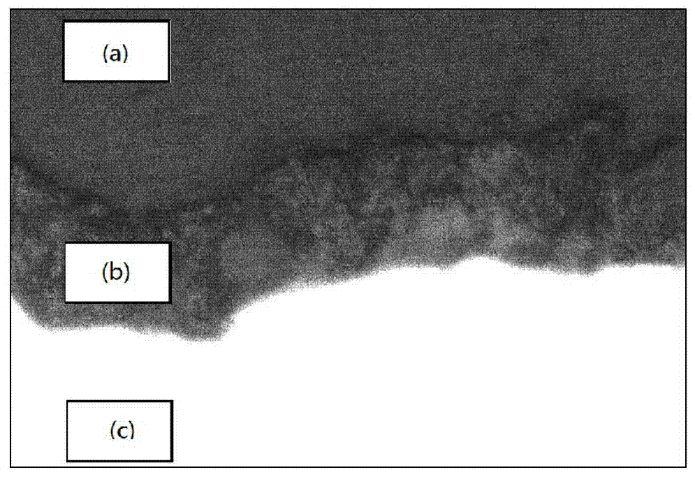
[0041] The metal substrate is selected as marine steel Q235B, and the surface film is ferric oxide, such as image 3 As...

Embodiment 2

[0046] (1) Select laser 1 as a Q-switched high-power neodymium glass solid laser, with a laser wavelength of 1064nm, a laser pulse width of 20ns, an output energy of 500mJ-20J, and a repetition frequency of 1Hz.

[0047] The photodetector 9 is selected as the photodiode of thorlab company, the model is DET10A / M, the rise time is less than 1ns, the response wavelength range is 200~1100nm, and the four-channel Yokogawa DL9140 oscilloscope is selected, the bandwidth is 1GHz, and the highest sampling rate is 2.5GS / s.

[0048] The focal length of the first focusing lens 4 is 1.5m, and the converging spot diameter is 5mm; the focal length of the second focusing lens 7 is 30cm, and the plasma flash signal is converged on the receiving surface of the photodetector;

[0049] The metal substrate is selected as a medical titanium alloy, the surface film is hydroxyapatite, and the film thicknesses of multiple samples are also different.

[0050] (2) Select the pulse laser energy as 10J, using su...

Embodiment 3

[0054] (1) The laser 1 is selected as a French high-power laser, the laser wavelength is 1064nm, the laser pulse width is 8ns, the output energy is 50mJ-12J, and the repetition frequency is 5Hz.

[0055] The photodetector 9 is selected as the photodiode of thorlab company, the model is DET10A / M, the rise time is less than 1ns, the response wavelength range is 200~1100nm, and the four-channel Yokogawa DL9140 oscilloscope is selected, the bandwidth is 1GHz, and the highest sampling rate is 2.5GS / s.

[0056] The focal length of the first focusing lens 4 is 1 m, and the converging spot diameter is 2 mm; the focal length of the second focusing lens 7 is 22.5 cm, and the plasma flash signal is concentrated on the receiving surface of the photodetector.

[0057] The metal substrate is pure aluminum, the surface film is black paint, and the film thicknesses of multiple samples are also different.

[0058] (2) Select the pulse laser energy to be 8J, use such as figure 1 The device shown and t...


PUM


Abstract

The invention provides a measurement device and a measurement method for film thickness, and belongs to the field of photoelectric detection. A laser is used for transmitting laser to be functioned on the surface of a material through a focus lens, so as to generate a laser plasma flashing signal; the laser passes through the focus lens and a band elimination filter, enters a photoelectric detector, and then is converted into a voltage signal processed by a processor through an oscilloscope; when the laser energy is large enough, the laser punctures a film material, appears a pit in a flashing intensity curve of a laser-induced plasma, and a linear relation is formed between the time of appearing the pit and the thickness of the film material. According to the measurement device for the film thickness provided by the invention, expensive micro instruments, such as an AFM (Atomic Force Microscope), cannot be needed, the environmental requirement is lower, no tool contact is caused in an integral measurement process, and the cost of changing the measurement tool can be saved and changed; furthermore, the measurement device is easy to operate and is convenient for a worker to use, and can be integrated on an automatic production line, thereby being likely to be popularized and applied in an industrial field.

Description

Technical field [0001] The invention belongs to the field of photoelectric detection, especially a device and method for measuring film thickness. Background technique [0002] Films are widely used in industry, and many performance indicators of films are related to their thickness. The measurement of film thickness is one of the basic inspection items in the film manufacturing industry. With the advancement of manufacturing technology and the miniaturization of instruments and equipment, micro-nano thin films endow the matrix materials with special physical and chemical properties and produce special application values. Therefore, the thickness detection of micro-nano thin films has also become a hot spot in scientific research. [0003] Films can be divided into two types: transparent and opaque. The high-precision measurement of transparent film thickness is mostly achieved by optical methods. For example, Chinese patent CN 102607435 B uses double slit interferometry to measu...

Claims


Application Information

Patent Timeline
Patent Type & Authority Patents(China)
IPC IPC(8): G01B11/06
Inventor 佟艳群石琳任旭东姚红兵张永康顾凌军岳震
Owner WANXIN OPTICAL GRP
Why Eureka
Try Eureka