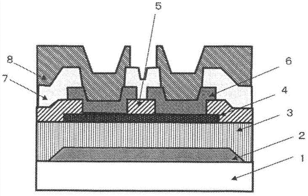
thin film transistor
A thin film transistor and protective film technology, applied in the manufacture of transistors, semiconductor devices, semiconductor/solid-state devices, etc., can solve problems such as characteristic degradation, and achieve the effect of excellent TFT characteristics
- Summary
- Abstract
- Description
- Claims
- Application Information
AI Technical Summary
Problems solved by technology
Method used
Image

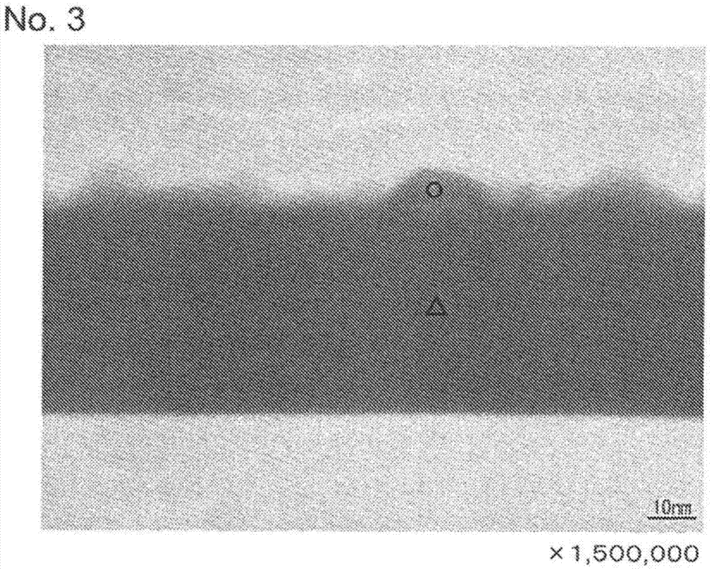
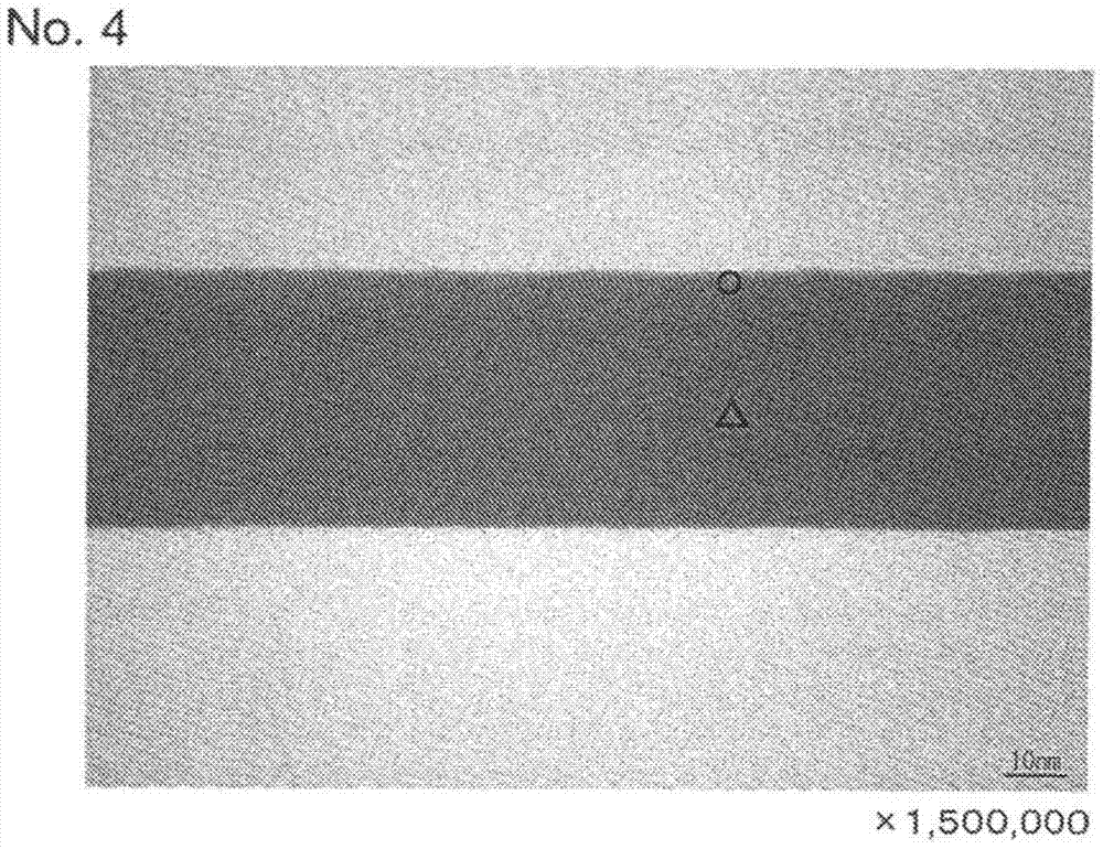
Examples
Embodiment
[0068] Hereinafter, the present invention will be described in more detail by citing the examples, but the present invention is not limited to the following examples, and can be appropriately modified and implemented within the scope of being able to adapt to the gist of the foregoing and the following. included in the technical scope of the present invention.
[0069] First, a Mo thin film (film thickness 100 nm) was formed on a glass substrate (EAGLE XG manufactured by Corning, diameter 100 mm×thickness 0.7 mm) as a gate electrode thin film, and patterned by a known method to obtain a gate electrode. The Mo thin film uses a pure Mo sputtering target, and is carried out by DC sputtering method under the conditions of film forming temperature: room temperature, film forming power: 300W, carrier gas: Ar, pressure: 2mTorr.
[0070] Next, as a gate insulating film, SiO 2 Film (200nm) was formed. The gate insulating film is formed by plasma CVD method in a carrier gas: SiH 4 an...
PUM
 Abstract
Description
Claims
Application Information