Cavity type film bulk acoustic resonator and its preparation method
A thin-film bulk acoustic wave and resonator technology, applied in impedance networks, electrical components, etc., can solve problems such as adverse effects of resonant structures, and achieve the effects of overcoming adverse effects, simplifying production processes, and reducing equipment costs
- Summary
- Abstract
- Description
- Claims
- Application Information
AI Technical Summary
Problems solved by technology
Method used
Image

Examples
Embodiment 1
[0055] A cavity-type film bulk acoustic resonator prepared by the following preparation method:
[0056] 1. A thin film structure layer is grown on the prepared substrate.
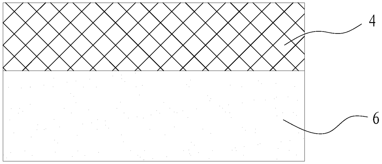
[0057] 1. Deposit a (0002) oriented single crystal aluminum nitride layer on the surface of the prepared substrate 6 made of silicon that has been cleaned and dried by standard RCA as the piezoelectric film 4. The thickness of the aluminum nitride layer depends on the actual application The frequency range of the decision, such as image 3 shown.
[0058] Among them, the piezoelectric film 4 of the single crystal aluminum nitride layer can be used at a trimethylaluminum (TMA) flow rate of about 50 sccm (ml / min in standard state), NH 3 The flow rate is about 3slm (standard state liter / min), the Ar flow rate is about 1slm, the substrate temperature is about 950°C, and the total pressure of the reaction chamber is about 40Tor. deposition) obtained by deposition.
[0059] 2. Using a radio frequency magnetr...
Embodiment 2
[0072] A cavity-type film bulk acoustic resonator prepared by the following preparation method:
[0073] 1. A thin film structure layer is grown on the prepared substrate.
[0074] 1. On the surface of the prepared substrate 6 made of silicon that has been cleaned and dried by standard RCA, use a radio frequency magnetron sputtering system to sputter on the surface of a single crystal aluminum nitride layer with a ZrN target (purity 99.995%) A layer of ZrN (zirconium nitride) is deposited as the top electrode 5 with a thickness of 100-300 nm.
[0075] 2. An aluminum nitride layer is deposited on the top electrode as the piezoelectric film 4, and the thickness of the aluminum nitride layer is determined according to the frequency range of the actual application. The aluminum nitride layer can be controlled at a TMA flow rate of 45 sccm (standard state ml / min), NH 3 The flow rate is about 2.5slm (standard state liter / min), the Ar flow rate is about 1slm, the substrate temperat...
PUM
 Abstract
Description
Claims
Application Information
 - R&D
- Intellectual Property
- Life Sciences
- Materials
- Tech Scout
- Unparalleled Data Quality
- Higher Quality Content
- 60% Fewer Hallucinations
Browse by: Latest US Patents, China's latest patents, Technical Efficacy Thesaurus, Application Domain, Technology Topic, Popular Technical Reports.
© 2025 PatSnap. All rights reserved.Legal|Privacy policy|Modern Slavery Act Transparency Statement|Sitemap|About US| Contact US: help@patsnap.com