Light-emitting diode epitaxial slice and preparation method thereof

A technology of light-emitting diodes and epitaxial wafers, applied in the direction of electrical components, circuits, semiconductor devices, etc., can solve the problems of difficult to meet the content requirements, difficult to meet a higher requirement, weak In-N bond strength, etc., and achieve high formation probability Effect

Active Publication Date: 2015-07-29
HC SEMITEK SUZHOU
View PDF4 Cites 13 Cited by
  • Summary
  • Abstract
  • Description
  • Claims
  • Application Information

AI Technical Summary

Problems solved by technology

[0005] In order to make the lattice constant of the stress release layer closer to the multi-quantum well layer, the content of the In component in the InGaN layer in the stress release layer is usually made to meet a higher requirement, and at the same time, in order to ensure the crystal quality of the stress release layer is usually A higher growth temperature will be used, but due to the weak strength of the In-N bond, too high a temperature will cause many In atoms to desorb from the growth surface of the InGaN layer and cannot be incorporated into the lattice, resulting in a stress release layer. The content of the In component in the InGaN layer is difficult to meet the requirements, and when the growth temperature is lower, only a small amount of In atoms that diffuse and move on the surface are captured by the dangling bonds of N to form In-N bonds, and the In atoms that diffuse and move In atoms form In droplets on the surface of the InGaN layer (that is, white spots directly observed from the epitaxial wafer), and the formation and growth process of In droplets is contradictory to the incorporation of In atoms into the lattice, which also makes the stress release layer The content of the In component in the InGaN layer is difficult to meet a higher requirement

Method used


Image

  • Light-emitting diode epitaxial slice and preparation method thereof
  • Light-emitting diode epitaxial slice and preparation method thereof
  • Light-emitting diode epitaxial slice and preparation method thereof

Examples


Embodiment 1

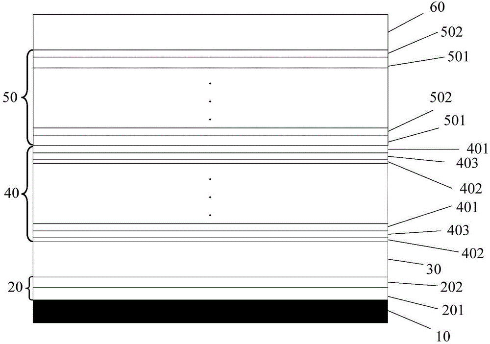
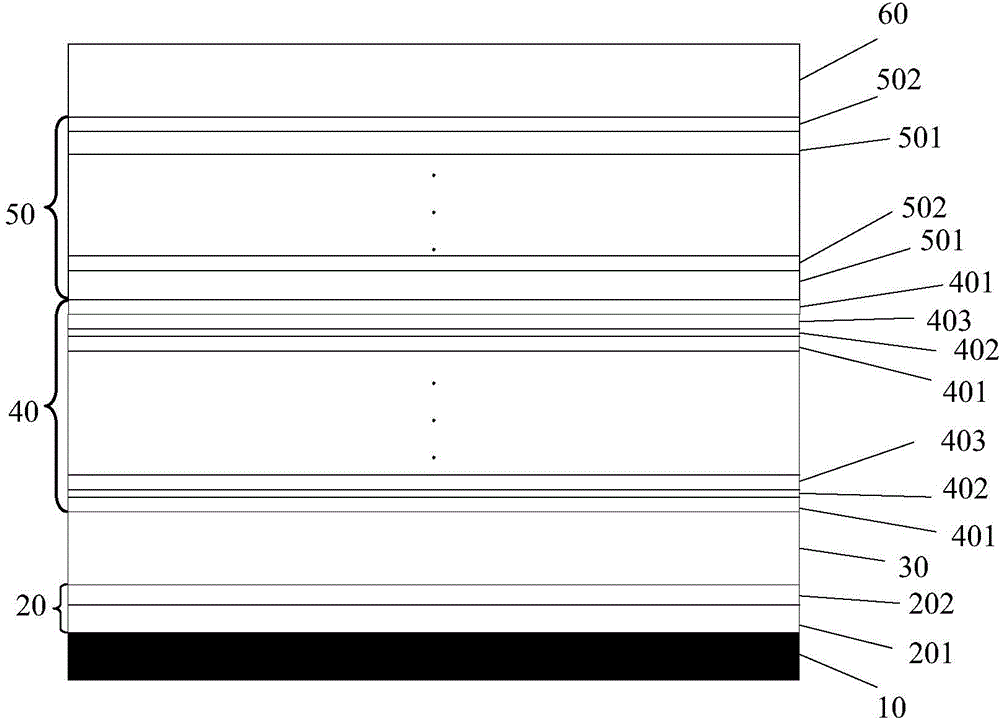
[0027] An embodiment of the present invention provides an epitaxial wafer of a light emitting diode, see figure 1 and figure 2 , the epitaxial wafer comprises a substrate 10, a buffer layer 20 grown on the substrate, an N-type layer 30, a stress release layer 40, a multi-quantum well layer 50 and a P-type layer 60, and the multi-quantum well layer 50 is a superlattice structure , each period of the MQW layer can include In y Ga 1-y N layer 501 and grown on In y Ga 1-y The GaN layer 502 on the N layer 501, 0x Ga 1-x N layer 403, 0

[0028] In this embodiment, the number of periods of the stress release layer 40 may be 2-20.

[0029] In the first implementation, see figure 1 , each period of the stress release layer 40 may include an InN layer 402, In grown on the InN layer 402 x Ga 1-x N layer 403 and grown on In x Ga 1-x The GaN layer 401 above the N layer 403 , that is, starting from the side of the N-type layer 30 , and the first InN layer 402 in the stress ...

Embodiment 2

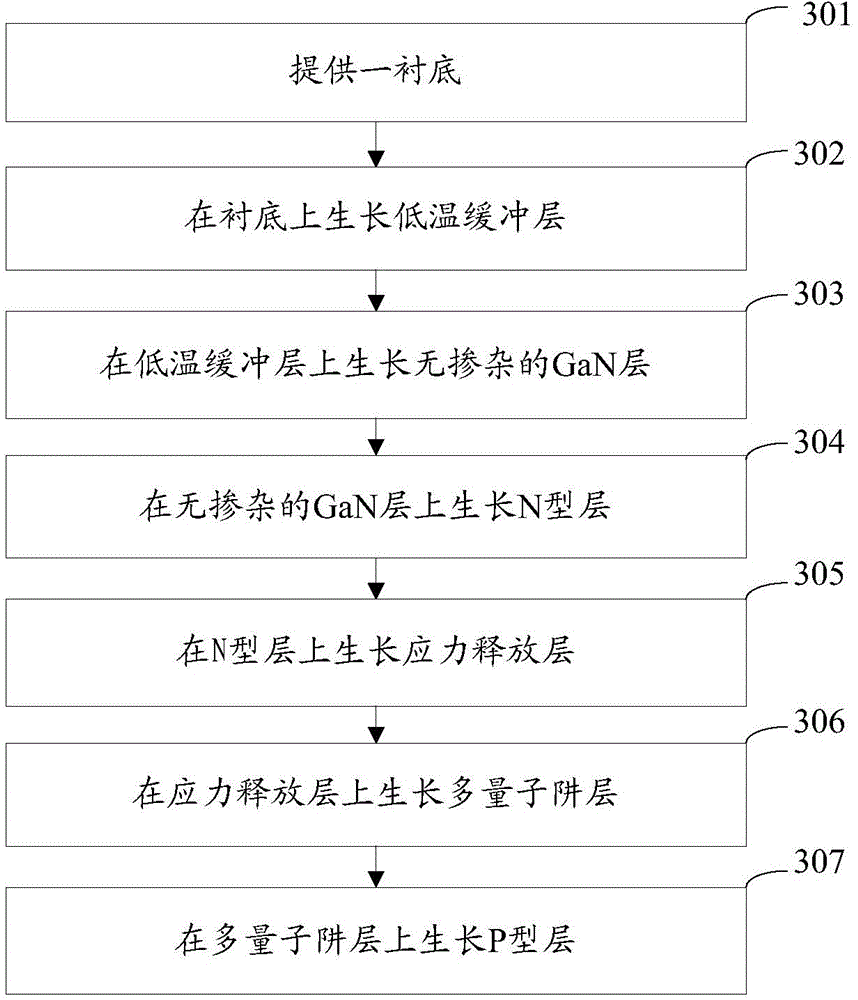
[0045] An embodiment of the present invention provides a method for preparing an epitaxial wafer of a light emitting diode, see image 3 , the method includes:

[0046] Step 301: Provide a substrate.

[0047] Specifically, the substrate may be a sapphire substrate, and may also be a Si substrate or a SiC substrate.

[0048] This step may also include cleaning the surface of the substrate. When it is realized, the sapphire substrate can be heated to 1110°C in a MOCVD (Metal-organic Chemical Vapor Deposition) reaction chamber, under hydrogen (H 2 ) atmosphere to anneal the sapphire substrate for 8 to 10 minutes to clean the surface of the substrate.

[0049] Step 302: growing a low-temperature buffer layer on the substrate.

[0050] Specifically, at a temperature of 540° C., a GaN layer with a thickness of about 30 nm is grown on the substrate as a low-temperature buffer layer.

[0051] Step 303: growing an undoped GaN layer on the low-temperature buffer layer.

[0052] Wh...


PUM


Abstract

The invention discloses a light-emitting diode epitaxial slice and a preparation method thereof, and belongs to the field of light-emitting diodes. The epitaxial slice comprises a substrate, a buffer layer, an N-type layer, a stress release layer, a multiple quantum well layer and a P-type layer, wherein the buffer layer, the N-type layer, the stress release layer, the multiple quantum well layer and the P-type layer sequentially grow on the substrate, the multiple quantum well layer is of a super-lattice structure, each cycle of the multiple quantum well layer includes an InyGa1-yN layer and a GaN layer, 0<y<1, the stress release layer is of a cycle structure, each cycle of the stress release layer includes a GaN layer, an InN layer and an InxGa1-xN layer growing on the InN layer, and 0<x<y. The InGaN layer grows on the InN layer in each cycle of the stress release layer, the formation probability of an In-N bond in the InGaN layer is high in rich In atmosphere, and In atoms can be more easily doped into a lattice to form the InGaN layer with high In component content.

Description

technical field [0001] The invention relates to the field of light-emitting diodes, in particular to an epitaxial wafer of a light-emitting diode and a preparation method thereof. Background technique [0002] In the development of the light-emitting diode industry, GaN, a wide bandgap (Eg>2.3eV) semiconductor material, is developing rapidly and is widely used in lighting, display screens, signal lights, backlight sources, toys and other fields. [0003] The epitaxial wafer of a traditional GaN-based light-emitting diode includes a sapphire substrate, a buffer layer grown sequentially on the sapphire substrate, an undoped GaN layer, an N-type layer, a multi-quantum well layer and a P-type layer. Wherein, the multi-quantum well layer is a superlattice structure, and each period includes alternately grown InGaN layers and GaN layers. Due to the large lattice mismatch between InGaN and GaN, there is a large stress at the heterointerface between the InGaN layer and the GaN l...

Claims


Application Information

Patent Timeline
Patent Type & Authority Applications(China)
IPC IPC(8): H01L33/12H01L33/04H01L33/00
CPCH01L33/0075H01L33/04H01L33/12
Inventor 李昱桦乔楠韩杰胡加辉魏世祯
Owner HC SEMITEK SUZHOU
Why Eureka
Try Eureka