Supercharge Your Innovation With Domain-Expert AI Agents!

A kind of Gan-based light-emitting diode epitaxial wafer and preparation method thereof

A technology of light-emitting diodes and epitaxial wafers, which is applied in the direction of semiconductor devices, electrical components, circuits, etc., can solve problems such as the decrease of luminous efficiency, and achieve the effects of increasing injection rate, reducing leakage, and improving recombination rate

Active Publication Date: 2018-10-09
HC SEMITEK CORP
View PDF5 Cites 0 Cited by
  • Summary
  • Abstract
  • Description
  • Claims
  • Application Information

AI Technical Summary

Problems solved by technology

[0006] In order to solve the problem that the luminous efficiency of existing LED chips decreases under the condition of high current density with the increase of operating current, the embodiment of the present invention provides a GaN-based light-emitting diode epitaxial wafer and its preparation method

Method used


Image

  • A kind of Gan-based light-emitting diode epitaxial wafer and preparation method thereof
  • A kind of Gan-based light-emitting diode epitaxial wafer and preparation method thereof

Examples


Embodiment 1

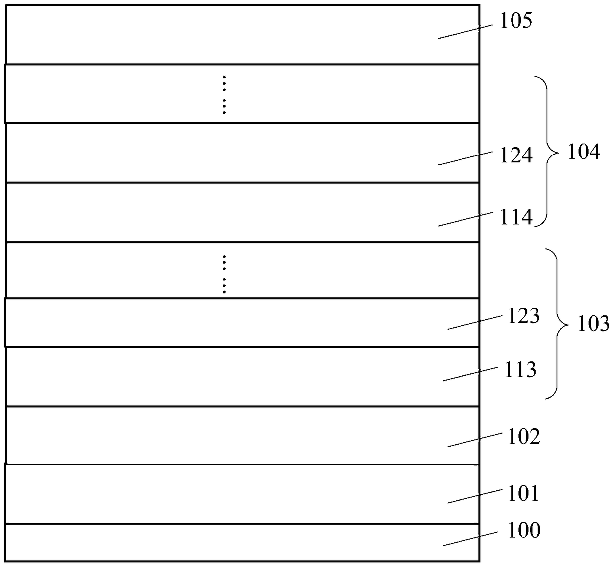
[0032] An embodiment of the present invention provides a GaN-based light-emitting diode epitaxial wafer, which is suitable for GaN-based LEDs with blue and green light waves, see figure 1 , the epitaxial wafer includes: a substrate 100, and a u-type GaN layer 101, an n-type GaN layer 102, a multi-quantum well layer 104, and a p-type GaN layer 105 covering the substrate 100 in sequence, the multi-quantum well layer 104 It includes: alternately grown InGaN well layers 114 and GaN barrier layers 124 .

[0033] The epitaxial wafer also includes: a barrier structure layer 103 disposed between the n-type GaN layer 102 and the multi-quantum well layer 104, the barrier structure layer 103 is an N-layer barrier structure, and each layer of barrier structure includes: The u-type GaN sublayer 113 and the p-type GaN sublayer 123, the value range of the thickness d1 of the u-type GaN sublayer 113 can be: 0nm

Embodiment 2

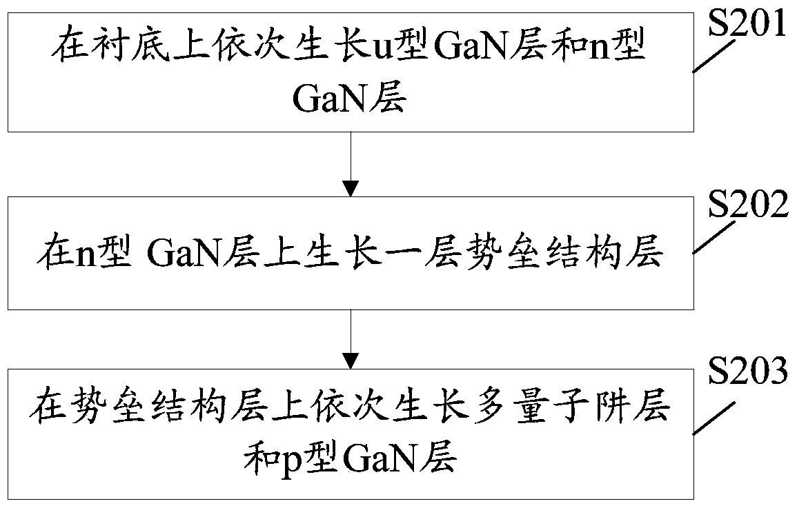
[0041] An embodiment of the present invention provides a GaN-based light-emitting diode epitaxial wafer preparation method, which is suitable for GaN-based LEDs with blue and green light waves, see figure 2 , the method includes:

[0042] Step S201, growing a u-type GaN layer and an n-type GaN layer sequentially on the substrate.

[0043] In this embodiment, the substrate may be a sapphire substrate.

[0044] Step S202, growing a barrier structure layer on the n-type GaN layer, the barrier structure layer includes an N-layer barrier structure, and each layer of barrier structure includes: a u-type GaN sublayer and a p-type GaN sublayer grown in sequence , the value range of the thickness d1 of the u-type GaN sublayer is: 0nm

[0045] Specifically, the p-type GaN sublayer may be a Mg-doped GaN sublayer, and the value range of the flow rate F ...


PUM


Abstract

The invention discloses a GaN-based light-emitting diode epitaxial wafer and a preparation method thereof, belonging to the technical field of semiconductors. The epitaxial wafer includes: a substrate, and a u-type GaN layer, an n-type GaN layer, a multi-quantum well layer, and a p-type GaN layer covering the substrate in sequence, and the epitaxial wafer also includes: The barrier structure layer between the GaN layer and the multi-quantum well layer, the barrier structure layer includes an N-layer barrier structure, and each barrier structure includes: a u-type GaN sub-layer and a p-type GaN sub-layer grown in sequence. The present invention forms a multi-layer energy barrier by adding a barrier structure layer composed of an N-layer barrier structure between the n-type GaN layer and the multi-quantum well layer, which can effectively reduce electrons in the n-type GaN layer under high current density. The injection rate of the multi-quantum well layer improves the recombination rate of electrons and holes in the multi-quantum well layer, thereby improving the luminous efficiency of the LED chip under high current density.

Description

technical field [0001] The invention relates to the technical field of semiconductors, in particular to a GaN-based light-emitting diode epitaxial wafer and a preparation method thereof. Background technique [0002] Light Emitting Diode (Light Emitting Diode, referred to as "LED") is a new solid-state lighting source with high efficiency and green environmental protection. It has the advantages of small size, light weight, long life, high reliability and low power consumption. Has been widely used. The existing GaN-based LED chip structure includes a substrate, a buffer layer, an n-type GaN layer, a multi-quantum well layer, a p-type GaN layer, and the like. [0003] During the working process of a GaN-based LED chip, the electrons generated in the n-type GaN layer and the holes generated in the p-type GaN layer migrate to the multi-quantum well layer under the action of an electric field, and radiative recombination occurs in the multi-quantum well layer , and then emit ...

Claims


Application Information

Patent Timeline
Patent Type & Authority Patents(China)
IPC IPC(8): H01L33/14H01L33/00
CPCH01L33/0066H01L33/007H01L33/0075H01L33/14H01L33/145
Inventor 孙玉芹王江波刘榕
Owner HC SEMITEK CORP
Features
  • R&D
  • Intellectual Property
  • Life Sciences
  • Materials
  • Tech Scout
  • Unparalleled Data Quality
  • Higher Quality Content
  • 60% Fewer Hallucinations
Learn More