
Eureka
For R&D, Eureka makes reading and utilizing patents & technical documents easy.
Eureka AIR
Designed for self-driven R&D workflows. Generate viable solutions, solve complex R&D challenges, empower your innovation with AI.

Eureka Materials
Designed for material experts only. Revolutionize your material R&D, from search, analyze, to developing new materials.

TechResearch
Generate reliable direction feasibility study reports for your R&D in just a few steps.

TechSeek
Discover and master advanced knowledge NOW. Basics, ideas, possibilities, all at once.

TechMind
As an expert in R&D Theories, TechMind can generates customized viable solutions instantly.

TechRisk
Analyze your overall solution with one click, know your potential R&D risks in advance.

TechMonitor
Get weekly tech updates, stay abreast of the latest tech innovations and key insights.
Transparent oled light extraction
A light extraction film, transparent and conductive technology, applied in optics, optical components, instruments, etc., can solve problems such as limited bottom emission design options
- Summary
- Abstract
- Description
- Claims
- Application Information
AI Technical Summary
Problems solved by technology
Method used
Image

Examples
example
[0054] All parts, percentages, ratios, etc. in the examples are by weight unless otherwise indicated. Solvents and other reagents used were purchased from Sigma-Aldrich Chemical Company, Milwaukee, WI unless otherwise noted.
[0055] Material
[0056]
preparation example
[0058] D510 Stabilized 50nm TiO 2 Preparation of Nanoparticle Dispersions
[0059] In the presence of SOLPLUS D510 and 1-methoxy-2-propanol, a grinding process was used to prepare TiO 2 TiO 2 Nanoparticle Dispersion. According to TiO 2 The weight of SOLPLUS D510 is added in an amount of 25% by weight. The mixture was premixed for 10 minutes using a DISPERMAT mixer (Paul N. Gardner Company, Inc., Pompano Beach, FL), and then subjected to the following conditions To use NETZSCH MiniCer grinder (Netzsch Premier Technologies, LLC., Exton, PA, Exton, Pennsylvania): 4300 rpm, YTZ grinding media of 0.2 mm, 250 ml / min flow rate. After 1 hour of grinding, TiO in 1-methoxy-2-propanol was obtained 2 Dispersion, white paste. Particles were sized to 50 nm (Z-average size) using a Malvern Instruments ZETASIZER Nano ZS (Malvern Instruments Inc, Westborough, MA).
[0060] Preparation of High Refractive Index Backfill Solution (HI-BF) :
[0061] 20g of D510 stabilized with 50...
example 1
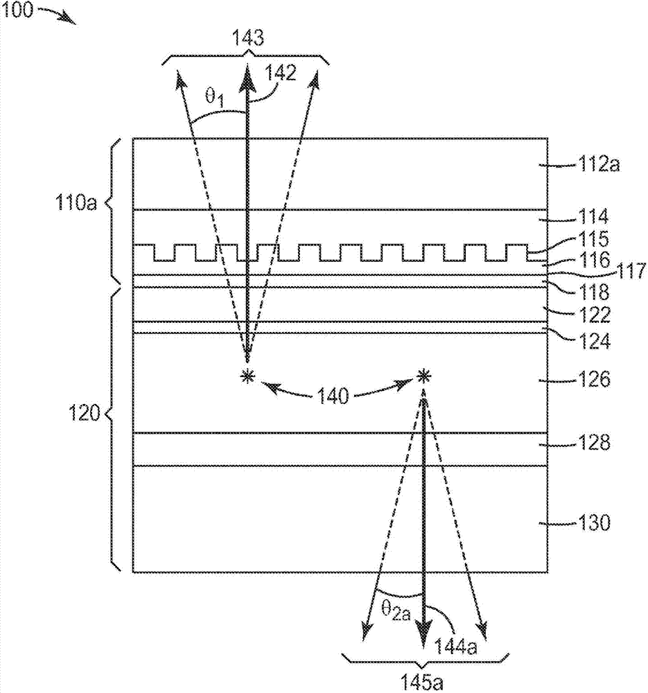
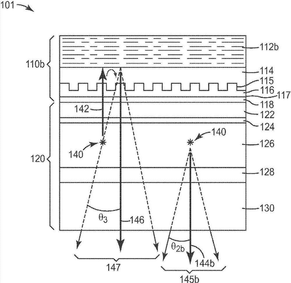
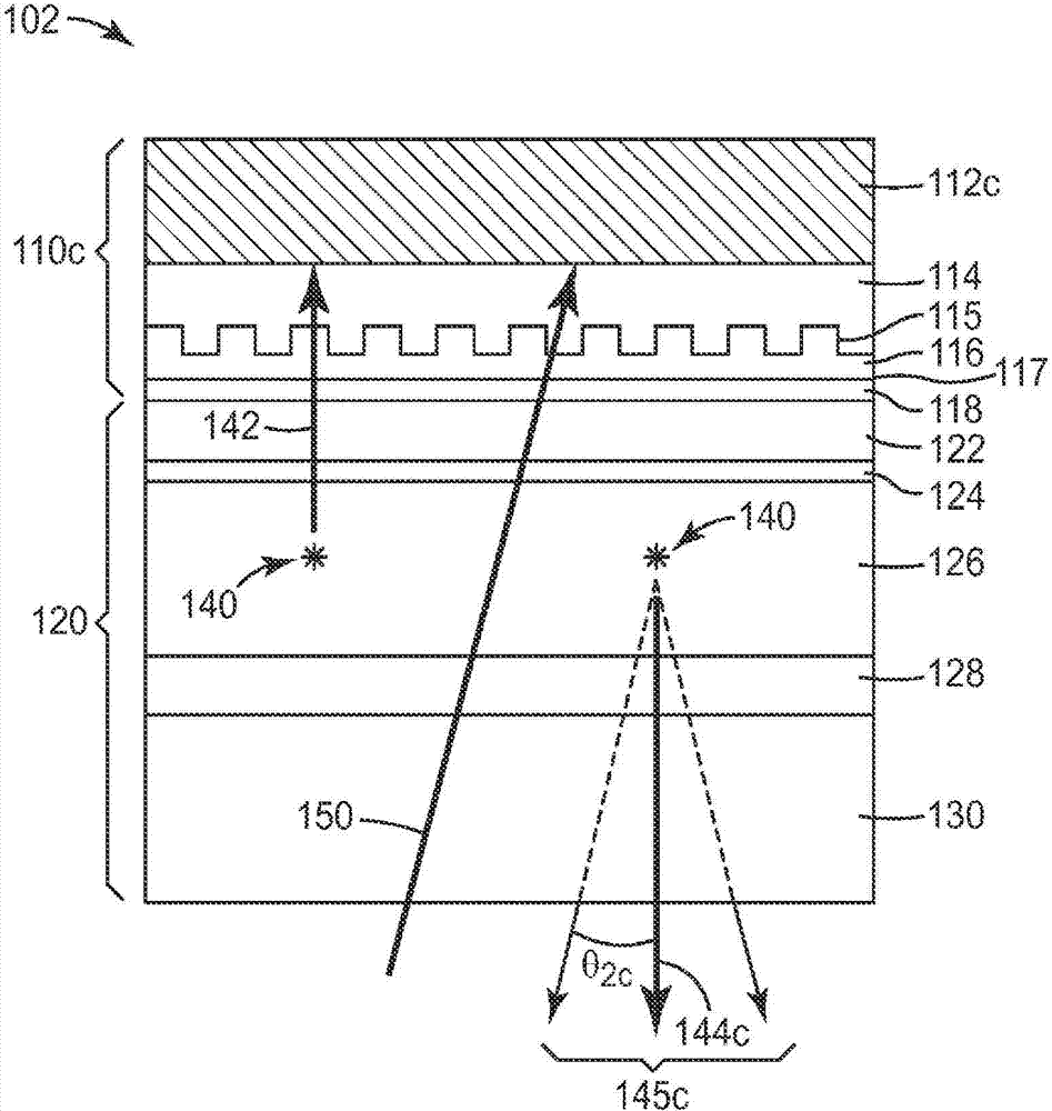
[0067] Using standard thermal deposition method at a base pressure of about 10 -6 Top-emitting (TE) OLED samples were constructed in a Torr vacuum system. Substrates with a 0.5 μm thick photoresist coating and an 80 nm ITO coating patterned to create four 5×5 mm square-arranged pixels were fabricated on ground float glass. A pixel defining layer (PDL) was applied to reduce the size of the squares to 4x4 mm and provide sharply defined pixel edges. Build the following structure:
[0068] Substrate / 80nm ITO lower electrode (cathode) / 20nm EIL / 25nm ETL / 30nm EML / 10nm HTL2 / 165nm HTL1 / 100nm HIL / 80nm ITO upper electrode (anode) / 200nm MoO3 cover layer ( CPL)
[0069] Among them, HIL, HTL, EML and ETL are respectively static for hole injection, hole transport, emission and electron transport layers. The top electrode is 80nm ITO, which is patterned through a shadow mask to align with the substrate layer. A pixel defining layer (PDL) was applied to reduce the size of the squares to 4...
PUM
| Property | Measurement | Unit |
|---|---|---|
| Thickness | aaaaa | aaaaa |
| Thickness | aaaaa | aaaaa |
| Thickness | aaaaa | aaaaa |
Abstract
Description
Claims
Application Information
 - R&D Engineer
- R&D Manager
- IP Professional
- Industry Leading Data Capabilities
- Powerful AI technology
- Patent DNA Extraction
Browse by: Latest US Patents, China's latest patents, Technical Efficacy Thesaurus, Application Domain, Technology Topic, Popular Technical Reports.
© 2024 PatSnap. All rights reserved.Legal|Privacy policy|Modern Slavery Act Transparency Statement|Sitemap|About US| Contact US: help@patsnap.com