LED packaging technical process based on iron substrate

A technology of LED packaging and process flow, applied in electrical components, circuits, semiconductor devices, etc., can solve the problems of rising LED packaging costs and high copper prices, and achieve the effects of increasing revenue, saving material costs, and reducing capital consumption.

Inactive Publication Date: 2015-08-05
CHANGZHI HONGYUAN PHOTOELECTRIC TECH
View PDF10 Cites 11 Cited by
  • Summary
  • Abstract
  • Description
  • Claims
  • Application Information

AI Technical Summary

Problems solved by technology

[0002] The LED substrate is mainly used as a medium for heat export between the LED chip and the system circuit board. By combining the process of wire bonding, eutectic or flip chip with the LED chip, the factor that affects the service life of the LED is mainly the evacuation of the heat of the LED chip. In order to achieve a good heat dissipation effect, traditional LEDs generally use copper substrate brackets. The thermal conductivity of copper is second only to silver among common metals, and it is an excellent conductor of heat. However, the price of copper is high, which leads to an increase in the cost of LED packaging.

Method used


Image

  • LED packaging technical process based on iron substrate

Examples


Embodiment 1

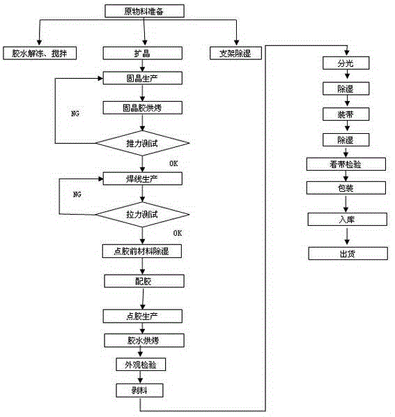
[0032] like figure 1 As shown, a kind of LED encapsulation technological process based on iron substrate of the present invention comprises the following steps:

[0033] a. Ultrasonic cleaning is used to clean the LED bracket. The LED bracket uses iron as the basic material, and the surface is nickel-plated and then silver-plated;

[0034] b. Dry and dehumidify the LED bracket, the dehumidification temperature is 150°C, and the dehumidification time is 2 hours;

[0035] c. Check the chip, whether there is mechanical damage and pitting on the surface of the material, whether the chip size and electrode size meet the process requirements, and whether the electrode pattern is complete;

[0036] d. Carry out the crystal expansion operation on the chip, and use the expansion machine to expand the film bonding the chip, so that the distance between the LED chips is stretched to about 0.6mm;

[0037] e. Thaw and stir the glue. Use syringe-type silver glue and insulating glue. The a...

Embodiment 2

[0056] In step i, the bonding power is 70mw; the bonding pressure is 60gms; the bonding time is 20ms; the bonding temperature is 130°C, and other steps are the same as in the first embodiment.

Embodiment 3

[0058] In step i, the bonding power is 110mw; the bonding pressure is 90gms; the bonding time is 10ms; the bonding temperature is 150°C, and other steps are the same as in the first embodiment.


PUM


Abstract

The invention discloses an LED packaging technical process based on an iron substrate, and belongs to the technical field of an LED packaging process, for solving the technical problem of providing an LED packaging technical process based on an iron substrate. For a lamp bead with power of 0.5 W below, the iron substrate is used to replace a copper substrate support, the heat dissipation requirement is met, the material cost can also be reduced, the economic benefits are improved, and after the surface of the iron substrate is plated with nickel, the iron substrate is also plated with silver so as to maintain the excellent performance of a product. The technical scheme employed by the invention is as follows: the LED packaging technical process based on the iron substrate comprises the steps of crystal expanding, crystal solidifying, baking, wire welding, dispensing, material stripping, light splitting, dehumidifying, bagging, examining and packaging. The LED packaging technical process is carried out on the substrate prepared by taking iron as a raw material. The LED packaging technical process based on the iron substrate can be applied to the technical field of the LED packaging process.

Description

technical field [0001] The invention discloses an iron substrate-based LED encapsulation process flow, belonging to the technical field of LED encapsulation process. Background technique [0002] The LED substrate is mainly used as a medium for heat export between the LED chip and the system circuit board. By combining the process of wire bonding, eutectic or flip chip with the LED chip, the factor that affects the service life of the LED is mainly the evacuation of the heat of the LED chip. In order to achieve a good heat dissipation effect, traditional LEDs generally use copper substrate brackets. Copper has a thermal conductivity second only to silver among common metals, and is an excellent conductor of heat. However, the price of copper is high, which leads to an increase in LED packaging costs. Contents of the invention [0003] The present invention overcomes the deficiencies in the prior art, and provides an LED packaging process based on an iron substrate. For lam...

Claims


Application Information

Patent Timeline
Patent Type & Authority Applications(China)
IPC IPC(8): H01L33/48H01L33/64
CPCH01L33/486H01L33/641H01L2933/0075
Inventor 徐龙飞
Owner CHANGZHI HONGYUAN PHOTOELECTRIC TECH
Why Eureka
Try Eureka