Multilayer printed circuit board and manufacturing method thereof

A technology of multi-layer printing and manufacturing methods, applied in the directions of printed circuit manufacturing, multi-layer circuit manufacturing, printed circuit, etc., which can solve problems such as distortion and inability to completely solve multi-layer printed wiring boards

Active Publication Date: 2015-08-05
MITSUI MINING & SMELTING CO LTD
View PDF11 Cites 3 Cited by
  • Summary
  • Abstract
  • Description
  • Claims
  • Application Information

AI Technical Summary

Problems solved by technology

[0014] However, in terms of the inventions disclosed in the above-mentioned patent documents 1 to 4, there are various problems in actual operation, and it is point

Method used


Image

  • Multilayer printed circuit board and manufacturing method thereof
  • Multilayer printed circuit board and manufacturing method thereof
  • Multilayer printed circuit board and manufacturing method thereof

Examples


Embodiment 1

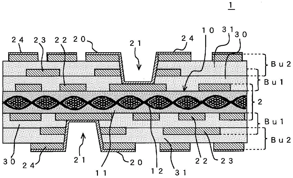
[0089] In this embodiment 1, through the following steps, manufactured such as Figure 6 Shown is a 10-layer multilayer printed wiring board.

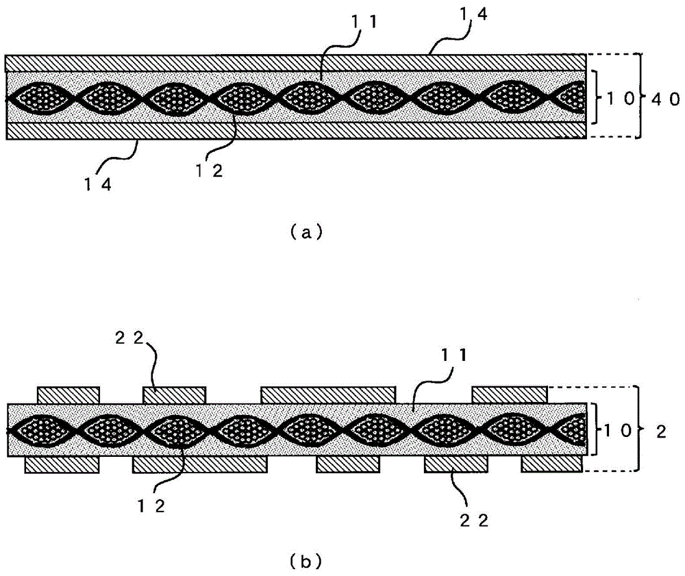
[0090] Step 1: In Example 1, prepared figure 2 (a) Copper-clad laminate with copper foil on both sides of the insulating layer in the state shown (copper foil thickness: 18 μm, insulating layer thickness: 60 μm, insulating layer: containing glass cloth, X-direction linear expansion rate: 14.0ppm / ℃, Y direction linear expansion rate 12.0ppm / ℃). Subsequently, the copper foil of the outer layer of the copper-clad laminate is etched to form predetermined inner-layer circuits 22 on both sides, thereby obtaining the following figure 2 The core substrate 2 in which the thickness of the insulating layer shown in (b) is 150 μm or less.

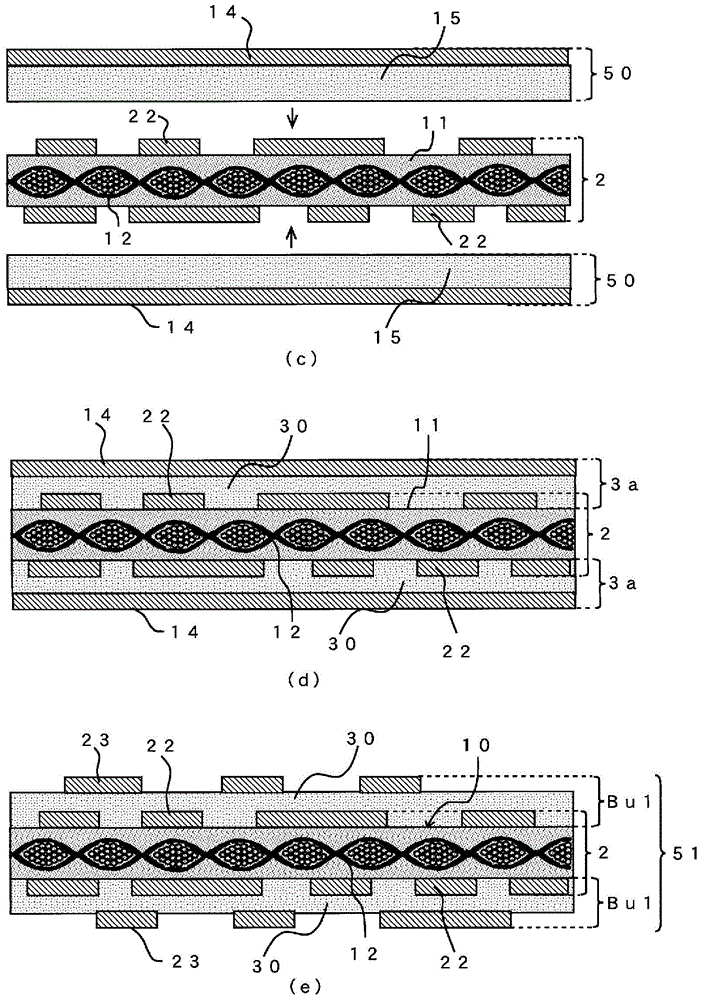
[0091] Process 2: In this process 2, if image 3 As shown in (c), the semi-cured resin layer 15 side of the copper foil 50 (thickness: 30 μm, copper foil thickness: 18 μm, semi-cured resin layer: resin f...

Embodiment 2

[0097] In this Example 2, through the same steps 1 to 4 as in Example 1, the following Figure 6 After the 10-layer multilayer printed wiring board shown, the warpage amount was measured in the same manner as in Example 1. Therefore, only the different parts will be described.

[0098] In this embodiment 2, just use the copper foil 50 (thickness: 30 μ m, copper foil thickness: 18 μ m, semi-cured resin layer: use epoxy resin, cyanate resin and bismaleyl resin) with semi-cured resin layer Resin film made of imide resin), for the insulating resin layer 32 of the first built-up wiring layer Bu1 to the third built-up wiring layer Bu3 formed through the same steps 1 to 3 as in Example 1, linear expansion in the X-Y direction The rate is 24ppm / °C, the ratio of the value of the X-direction linear expansion coefficient (Bx) to the Y-direction linear expansion coefficient (By) of the insulating resin layer is [Bx] / [By]=1.0, and the tensile strength at 25°C is The elastic modulus is 8....


PUM

PropertyMeasurementUnit
Thicknessaaaaaaaaaa
Tensile modulus of elasticityaaaaaaaaaa
Thicknessaaaaaaaaaa

Abstract

The purpose of the present invention is to provide a multilayer printed circuit board which mitigates the problems of "warping," "twisting" and "changing size" seen in printed circuit boards obtained by the conventional build-up method, and to provide a manufacturing method thereof. In order to achieve this purpose, a multilayer printed circuit board is adopted which is provided with two more build-up wiring layers on both sides of a core substrate, wherein said core substrate is provided with an inner layer circuit on both sides of the skeletal material-containing insulation layer, the insulation layer being 150μm thick or less, wherein the X-Y direction linear expansion coefficient of the skeletal material-containing insulation layer is 0ppm/°C-20ppm/°C, a first build-up wiring layer and a second build-up wiring layer provided on both sides of the core substrate comprise a copper circuit layer and an insulating resin layer having a X-Y direction linear expansion coefficient of 1ppm/°C-50ppm/°C, and the relation holds that the ratio of the value of the X-direction linear expansion coefficient (Bx) and the value of the Y-direction linear expansion coefficient (By) of the insulating resin layer is 0.9-1.1.

Description

technical field [0001] The present invention relates to a multilayer printed wiring board and its manufacturing method. In particular, it relates to a multilayer printed wiring board manufactured by a build-up method. Background technique [0002] Conventionally, multilayer printed wiring boards have been widely used for purposes such as increasing the signal transmission speed and reducing the mounting area as a printed wiring board. This multilayer printed wiring board is used to mount various electronic components. When mounting electronic components on this multilayer printed wiring board, various methods such as reflow soldering and wire bonding are used. In this case, if "warping", "twisting" and "dimensional change" occur in the multilayer printed wiring board, it will not be possible to mount favorable electronic components, so it is not preferable. In particular, when the build-up method (build-up method) is used as the manufacturing method of the multilayer prin...

Claims


Application Information

Patent Timeline
IPC IPC(8): H05K3/46
CPCH05K3/4602H05K3/4652H05K2201/09518H05K1/0271H05K1/0366H05K2201/068
Inventor 大泽和弘松岛敏文桑子富士夫
Owner MITSUI MINING & SMELTING CO LTD
Why Eureka
Try Eureka