Zr‑sb‑te series phase change material for phase change memory and preparation method thereof
A phase change memory and phase change material technology, applied in the field of microelectronics, can solve the problems of poor data retention and low thermal stability of phase change materials, and achieve the effects of high deposition state stability and good crystallization speed.
- Summary
- Abstract
- Description
- Claims
- Application Information
AI Technical Summary
Problems solved by technology
Method used
Image
Examples
Embodiment 1
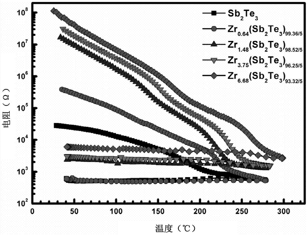
[0032] In this example, by preparing Zr 100-x-y (Sb 2 Te 3 ) (x+y) / 5Phase change material, and it is tested to further illustrate a technical solution of the present invention. Concrete preparation scheme is as follows:
[0033] (1) Using the dual-target co-sputtering method in magnetron sputtering to simultaneously prepare Zr on silicon substrates and thermally oxidized silicon substrates 100-x-y Sb x Te y Phase change materials, where 0<100-x-y<20, 0.5≤x / y≤4. The prepared Zr-Sb-Te series phase change materials are thin film materials, and the film thickness can be controlled at 100-250nm by adjusting the long film time.
[0034] Specifically, the following steps are included: under an argon atmosphere, using Sb 2 Te 3 Alloy target and Zr elemental target two target co-sputtering, in which, Sb 2 Te 3 The alloy target adopts DC power supply, and the Zr simple substance target adopts radio frequency power supply; the atomic percentage of Zr is adjusted by changing th...
Embodiment 2
[0046] In this example, by preparing Zr 100-x-y (Sb 2 Te) (x+y) / 3 Phase change material, and it is tested to further illustrate another technical solution of the present invention. Concrete preparation scheme is as follows:
[0047] (1) Using the three-target co-sputtering method in magnetron sputtering to simultaneously prepare Zr on silicon substrates and thermally oxidized silicon substrates 100-x-y Sb x Te y Phase change materials, where 0<100-x-y<20, 0.5≤x / y≤4.
[0048] Specifically, the following steps are included: under an argon atmosphere, using Sb 2 Te 3 Alloy target, Zr elemental target and Sb elemental target three target co-sputtering, wherein, Sb 2 Te 3The alloy target and the Sb elemental target adopt DC power supply, and the Zr elemental target adopts radio frequency power supply; the atomic percentage of Zr is adjusted by changing the radio frequency power, and the composition ratio of Sb and Te is adjusted by changing the DC power of the Sb elemental...
PUM
| Property | Measurement | Unit |
|---|---|---|
| thickness | aaaaa | aaaaa |
Abstract
Description
Claims
Application Information
 - R&D
- Intellectual Property
- Life Sciences
- Materials
- Tech Scout
- Unparalleled Data Quality
- Higher Quality Content
- 60% Fewer Hallucinations
Browse by: Latest US Patents, China's latest patents, Technical Efficacy Thesaurus, Application Domain, Technology Topic, Popular Technical Reports.
© 2025 PatSnap. All rights reserved.Legal|Privacy policy|Modern Slavery Act Transparency Statement|Sitemap|About US| Contact US: help@patsnap.com


