

Single granule layer nanometer diamond film with strong Si-V luminescence, and production method thereof
A nano-diamond and single-particle technology, applied in nanotechnology, nanotechnology, nanotechnology, etc. for materials and surface science, can solve problems that do not involve single-particle layer nanodiamond films, and achieve Si-V luminescence performance Unstable, simple solution, and the effect of improving Si-V luminous intensity
- Summary
- Abstract
- Description
- Claims
- Application Information
AI Technical Summary
Problems solved by technology
Method used
Image

Examples
Embodiment 1
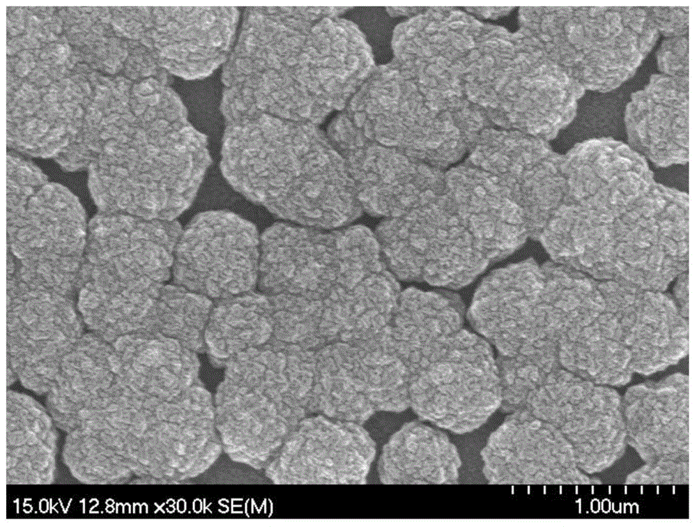
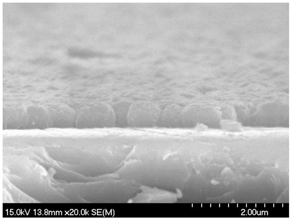
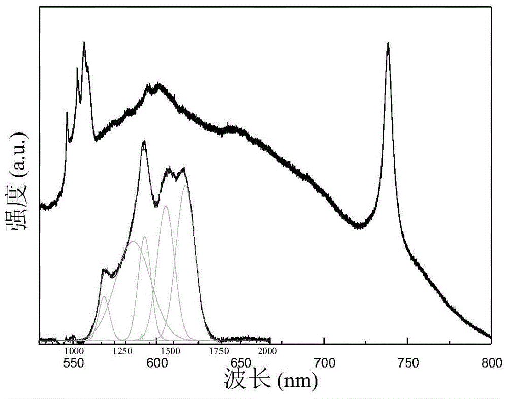
[0030] Polish the monocrystalline silicon wafer with nano-scale diamond powder, and the grinding time is about half an hour. Polished silicon wafers were ultrasonically cleaned with deionized water and acetone in turn, dried, and used as substrates for the growth of nano-diamond films. The hot wire chemical vapor deposition method (chemical vapor deposition equipment was purchased from Shanghai Jiaoyou Diamond Coating Co., Ltd., model JUHF CVD 001) was used, acetone was used as the carbon source, and acetone was brought into the reaction chamber by hydrogen bubbling. The flow ratio to acetone is 200:90, the reaction power is 2200W, the distance between the hot wire and the substrate silicon wafer is 7mm, and the working pressure is 1.63Kpa; no bias is applied during the reaction, and the preparation time is 15 minutes; after the growth , the temperature of the sample is cooled under the condition of no hydrogen, and a single particle layer nano-diamond film with a thickness of...
Embodiment 2
[0037] The monocrystalline silicon wafer is polished with nanometer diamond powder, and the polishing time is about half an hour. The polished silicon wafers were washed with deionized water and acetone in an ultrasonic machine, dried, and used as substrates for the growth of nano-diamond films. The hot wire chemical vapor deposition method (chemical vapor deposition equipment was purchased from Shanghai Jiaoyou Diamond Coating Co., Ltd., model JUHF CVD 001) was used, acetone was used as the carbon source, and acetone was brought into the reaction chamber by hydrogen bubbling. The flow ratio with acetone is 200:90, the reaction power is 2200W, the distance between the hot wire and the substrate silicon wafer is 7mm, the working pressure is 1.63Kpa; no bias is applied during the reaction, and the film preparation time is 15 minutes. After the growth is finished, the temperature of the sample is cooled under the condition of not flowing hydrogen, and a single particle layer nano...
Embodiment 3
[0041] The monocrystalline silicon wafer is polished with nanometer diamond powder, and the polishing time is about half an hour. The polished silicon wafers were washed with deionized water and acetone in an ultrasonic machine, dried, and used as substrates for the growth of nano-diamond films. The hot wire chemical vapor deposition method (chemical vapor deposition equipment purchased from Shanghai Jiaoyou Diamond Coating Co., Ltd., model JUHF CVD 001) was used, with acetone as the carbon source, and acetone was brought into the reaction chamber by hydrogen bubbling. , The flow ratio of hydrogen gas is 200:90, the power is 2200W, the distance between the hot wire and the substrate silicon wafer is 7mm, and the working pressure is 1.63Kpa; no bias is applied during the reaction process, and the preparation time is 15 minutes; after the growth is over, The temperature of the sample is lowered and cooled under the condition of not flowing hydrogen, and a single particle layer n...
PUM
| Property | Measurement | Unit |
|---|---|---|
| Thickness | aaaaa | aaaaa |
| Thickness | aaaaa | aaaaa |
| Thickness | aaaaa | aaaaa |
Abstract
Description
Claims
Application Information