A Raman test system and test method for in-situ testing LED stress

A technology of in-situ testing and testing system, which is applied in the direction of measuring the change force of optical properties of materials when they are stressed, and can solve problems such as high Raman spectroscopy, weak Raman scattering signal intensity, and inability to solve stress testing. , to avoid interference and improve the signal-to-noise ratio

Active Publication Date: 2017-11-07
XIAMEN UNIV
View PDF6 Cites 0 Cited by
  • Summary
  • Abstract
  • Description
  • Claims
  • Application Information

AI Technical Summary

Problems solved by technology

The stress test of traditional semiconductors generally adopts Raman test system, but because the Raman scattering signal intensity is weak, it is 2 to 3 orders of magnitude lower than the fluorescence intensity of LED under current injection conditions, resulting in the Raman signal of the traditional Raman test system It will be overwhelmed by the fluorescence spectrum of the LED, and the Raman spectrum with a high signal-to-noise ratio cannot be obtained. Therefore, the stress test of the LED under current injection cannot be performed using the traditional Raman test system
[0003] In view of the fact that the existing Raman test system cannot solve the LED stress test under the condition of current injection, and it is difficult to detect and analyze the influence of stress on the performance of LEDs, it is necessary to propose a new method for in-situ testing of LED stress

Method used


Image

  • A Raman test system and test method for in-situ testing LED stress
  • A Raman test system and test method for in-situ testing LED stress
  • A Raman test system and test method for in-situ testing LED stress

Examples


Embodiment Construction

[0022] The present invention will be further described in detail below in conjunction with the accompanying drawings and specific embodiments.

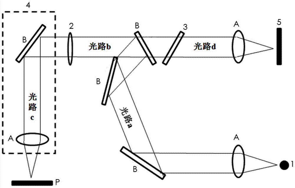
[0023] see figure 1 , the embodiment of the Raman test system for in-situ testing of LED stress in the present invention is provided with a laser 1, an optical path system a / b / c / d, a long-wave pass or band-pass filter 2, a Raman filter 3, a microscope 4, and a CCD 5 The long-wave pass or bandpass filter 2 is located at the front end of the microscope light path in the Raman light path, the rear end of the microscope light path, the front end of the Raman filter, the rear end of the Raman filter or the front end of the CCD, etc., preferably the rear end of the microscope light path, And combined with a laser whose wavelength is far away from the LED light emission spectrum.

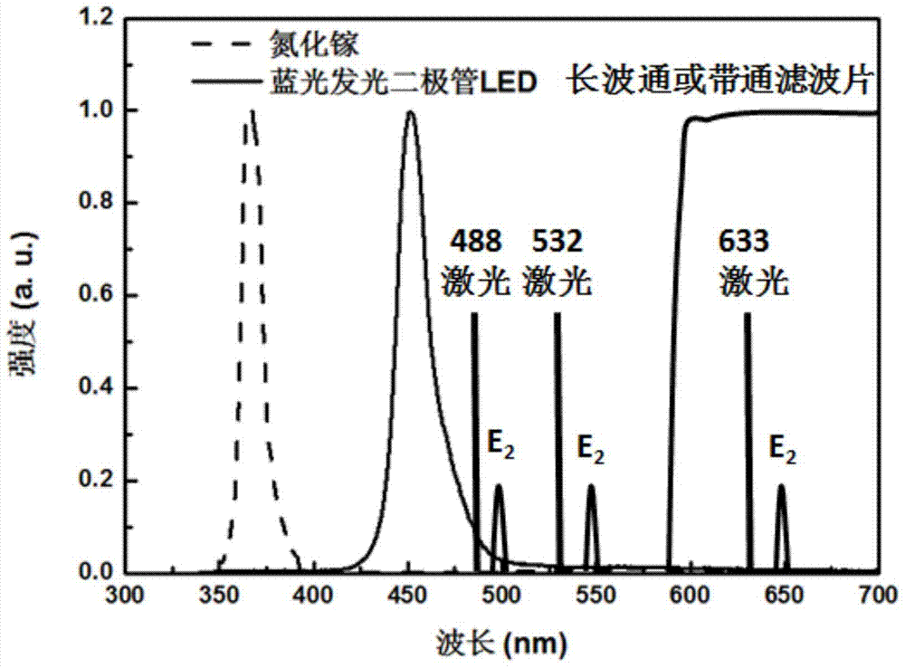
[0024] The long-wave pass or band-pass filter 2 allows signals with a wavelength greater than 600nm to be filtered, and the long-wave pass or band-pass filter is...


PUM

PropertyMeasurementUnit
wavelengthaaaaaaaaaa

Abstract

A Raman test system and test method for in-situ testing of LED stress, the test system is equipped with a laser, an optical system, a long-wave pass or band-pass filter, a Raman filter, a microscope, a CCD; a long-wave pass or a band-pass filter It is set at the front end of the microscope optical path, the rear end of the microscope optical path, the front end of the Raman filter, the rear end of the Raman filter or the front end of the CCD, etc. in the Raman optical path, and is combined with a laser whose wavelength is far away from the LED emission spectrum. Test method: first use the microscope to adjust the position of the sample to make the sample focus; turn off the light source of the microscope, turn on the laser, the laser is used to emit the laser light required for Raman testing, the optical path system transmits the input and output signals of the laser, and reflects the light After signal processing and filtering by Raman filter, the final signal is detected by CCD. Improve the signal-to-noise ratio of the Raman signal and realize the in-situ test of LED stress under different current injection conditions.

Description

technical field [0001] The invention relates to semiconductor optoelectronics and semiconductor testing, in particular to a Raman testing system and testing method for in-situ testing LED stress. Background technique [0002] Light-emitting diodes (LEDs) generally use heteroepitaxy. In the case of current injection, due to the differences in lattice constants, thermal expansion coefficients, and the influence of current and voltage on the lattice between materials, etc. [1],[2],[3] ,, the stress of the LED will change, which will cause problems such as the decrease of the luminous intensity of the LED, efficiency droop, luminous wavelength shift, and package mismatch. [4],[5] . The stress test of traditional semiconductors generally adopts Raman test system, but because the Raman scattering signal intensity is weak, it is 2 to 3 orders of magnitude lower than the fluorescence intensity of LED under current injection conditions, resulting in the Raman signal of the tradition...

Claims


Application Information

Patent Timeline
Patent Type & Authority Patents(China)
IPC IPC(8): G01L1/24
Inventor 康俊勇郑锦坚林伟
Owner XIAMEN UNIV
Why Eureka
Try Eureka