A vertical interconnection structure with electromagnetic shielding effect and manufacturing method thereof
A vertical interconnection, electromagnetic shielding technology, applied in circuits, electrical components, electrical solid devices, etc., can solve problems such as electromagnetic leakage, achieve small size, solve electromagnetic leakage, and good heat dissipation effect.
- Summary
- Abstract
- Description
- Claims
- Application Information
AI Technical Summary
Problems solved by technology
Method used
Image
Examples
Embodiment 1
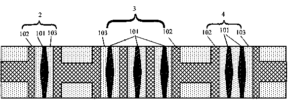
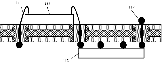
[0054] to combine Figure 1-Figure 4 , this embodiment describes in detail the vertical interconnection structure with electromagnetic shielding performance of the present invention, which may include any one or more of a single-channel vertical interconnection structure 2, a multi-channel vertical interconnection structure 3, and a differential vertical interconnection structure , this embodiment includes a single-channel vertical interconnection structure 2, a multi-channel vertical interconnection structure 3 and a differential vertical interconnection structure 4 as an example, and its structural diagram is as follows figure 1 As shown, the top view is as figure 2As shown, the single-channel vertical interconnect structure 2 includes a solid metal via 101, an annular metal shielding layer 102 surrounding the solid metal via 21, and an annular metal shield between the solid metal via 101 and the metal shielding layer 102. The insulating dielectric metal oxide 103; the mul...
Embodiment 2
[0061] combine Figure 5 - Fig. 6, this embodiment describes in detail the fabrication method of the vertical interconnection structure with electromagnetic shielding function of the present invention, its flow chart is as follows Figure 5 shown, including the following steps:
[0062] S11: providing a metal substrate 1, coating a layer of photosensitive material on the upper and lower surfaces of the metal substrate 1 for the first time, performing double-sided photolithography for the first time, and forming a pattern mask 11 of a vertical interconnection structure;
[0063] S12: Perform dense anodic oxidation on the metal substrate after forming the pattern mask of the vertical interconnection structure, and form a dense metal oxide layer in the area not covered by the pattern mask of the vertical interconnection structure;
[0064] S13: Use chemical etching and sputter etching to remove the pattern mask of the vertical interconnection structure, coat a layer of photosens...
PUM
 Abstract
Description
Claims
Application Information


