

Preparation method of microarray structure on basis of DLP (digital light processing) technology and chemical vapor deposition
A chemical vapor deposition and vapor deposition technology, applied in gaseous chemical plating, metal material coating process, coating and other directions, to achieve the effect of large selection of materials, simple equipment, and high recoverability
- Summary
- Abstract
- Description
- Claims
- Application Information
AI Technical Summary
Problems solved by technology
Method used
Image

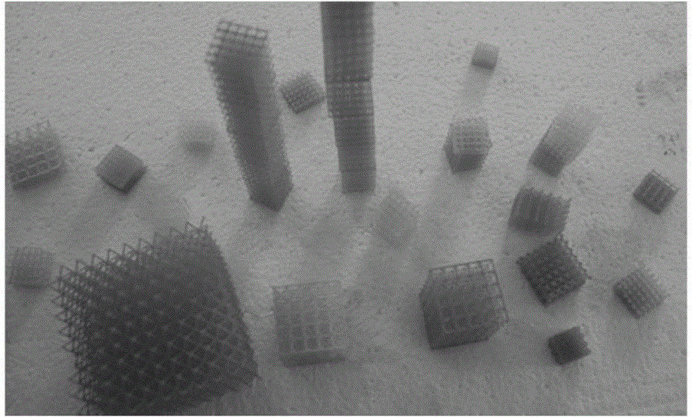
Examples
specific Embodiment approach 1
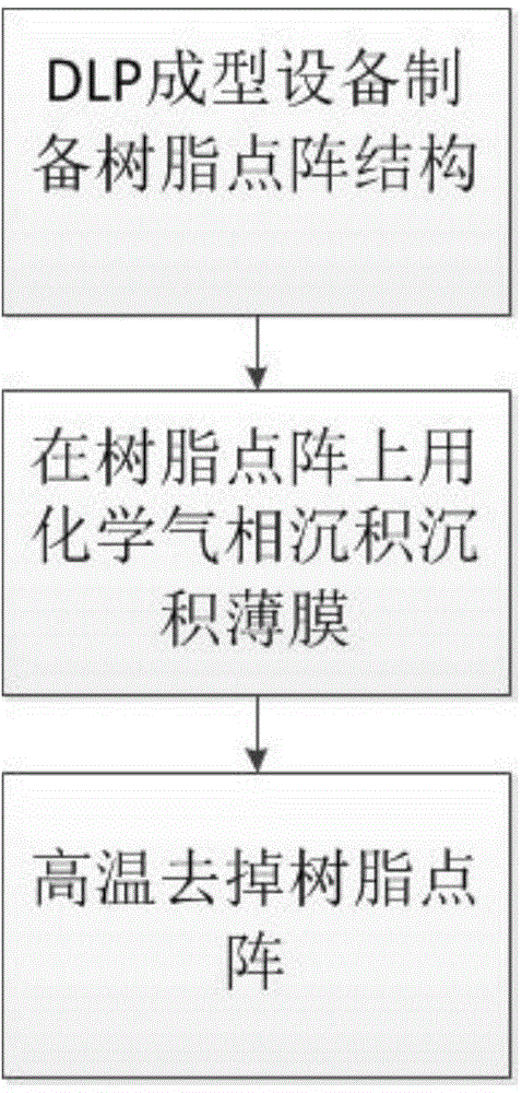
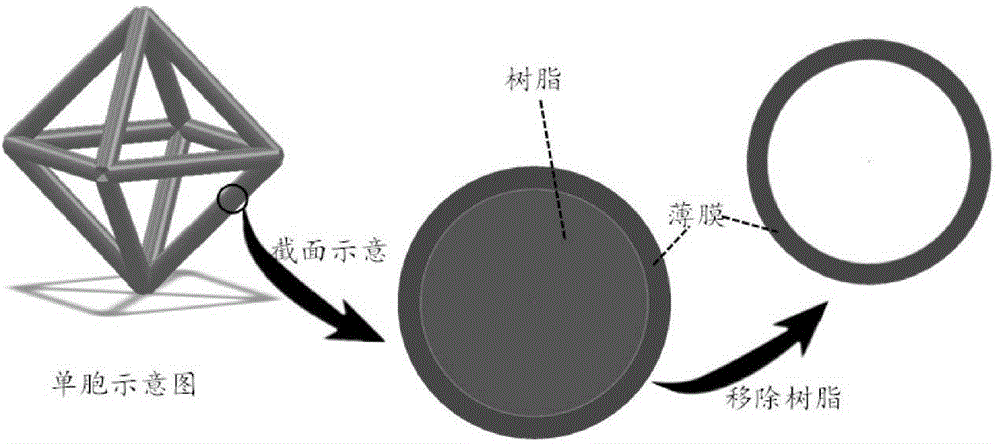
[0029] Specific embodiment one: a kind of micro lattice structure preparation method based on DLP technology and chemical vapor deposition of the present embodiment, it comprises following preparation steps:
[0030] Step 1: Use DLP molding equipment to prepare a dot matrix of photosensitive resin material;
[0031] Step 2: forming a thin film on the photosensitive resin material structure by chemical vapor deposition;
[0032] Step 3: after removing the photosensitive resin on the film of step 2, a lattice structure is obtained;
[0033] Wherein, the chemical vapor deposition described in the step 2, the specific operation steps are as follows:
[0034] 1) Put the photosensitive resin lattice obtained in step 1 into the vapor deposition chamber, and replace the air in the vapor deposition chamber with an inert gas with a flow rate of 100mL / min for 5 minutes, and then heat the temperature of the vapor deposition chamber to 100°C-190°C , stop the inert purge gas after maintai...
specific Embodiment approach 2
[0038] Specific embodiment 2: The difference between this embodiment and specific embodiment 1 is that in step 1, the DLP molding equipment includes a digital projector, an LCD light source or an LED light source as a curing light source; the process parameters of the DLP molding equipment are: single layer The thickness is 10-150 microns, the curing time of the first layer is 20-60s, and the curing time of the single layer is 3-20s; the input file is in STL format. Others are the same as in the first embodiment.
specific Embodiment approach 3
[0039] Embodiment 3: This embodiment is different from Embodiment 1 in that: the gasification reactant is nickel carbonyl. Others are the same as in the first embodiment.
PUM
| Property | Measurement | Unit |
|---|---|---|
| diameter | aaaaa | aaaaa |
| length | aaaaa | aaaaa |
| thickness | aaaaa | aaaaa |
Abstract
Description
Claims
Application Information