Quantum dot LED with dual photonic crystal structure

A technology of quantum dot luminescence and crystal structure, which is applied in semiconductor devices, electrical components, circuits, etc., and can solve problems such as the application of quantum dot LEDs that have not yet been seen

Active Publication Date: 2015-10-07
SOUTHEAST UNIV
View PDF4 Cites 13 Cited by
  • Summary
  • Abstract
  • Description
  • Claims
  • Application Information

AI Technical Summary

Problems solved by technology

So far, the method of simultaneously setting two or more photonic crystal structures in LEDs is extremely rare even in ordinary quantum well LEDs, and the application of gas in quantum dot LEDs has not yet been seen.

Method used


Image

  • Quantum dot LED with dual photonic crystal structure
  • Quantum dot LED with dual photonic crystal structure
  • Quantum dot LED with dual photonic crystal structure

Examples


Embodiment Construction

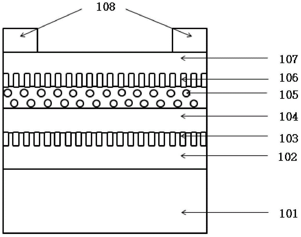
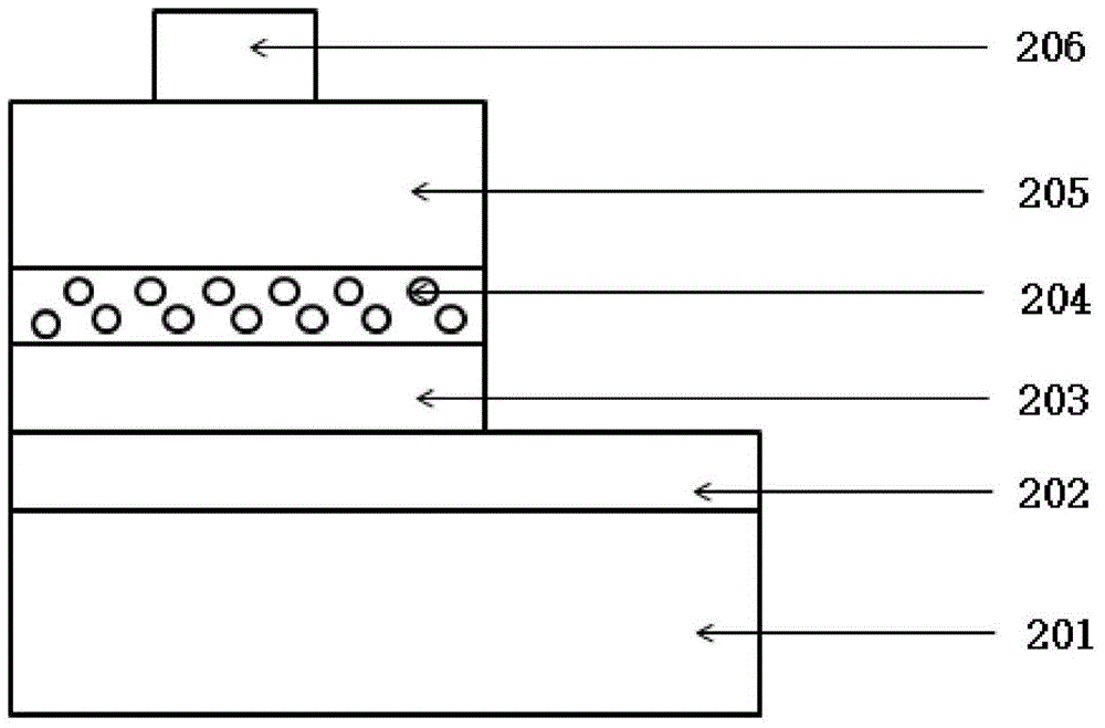
[0022] Such as figure 1 As shown, a quantum dot light-emitting diode with a two-photon crystal structure provided by the present invention, its constituent elements include: a substrate 101, a hole injection layer 102, a photonic crystal 103, and a hole transport layer from bottom to top 104, a quantum dot active region 105, a photonic crystal 2 106, an electron transport layer 107, and an electron injection layer 108.

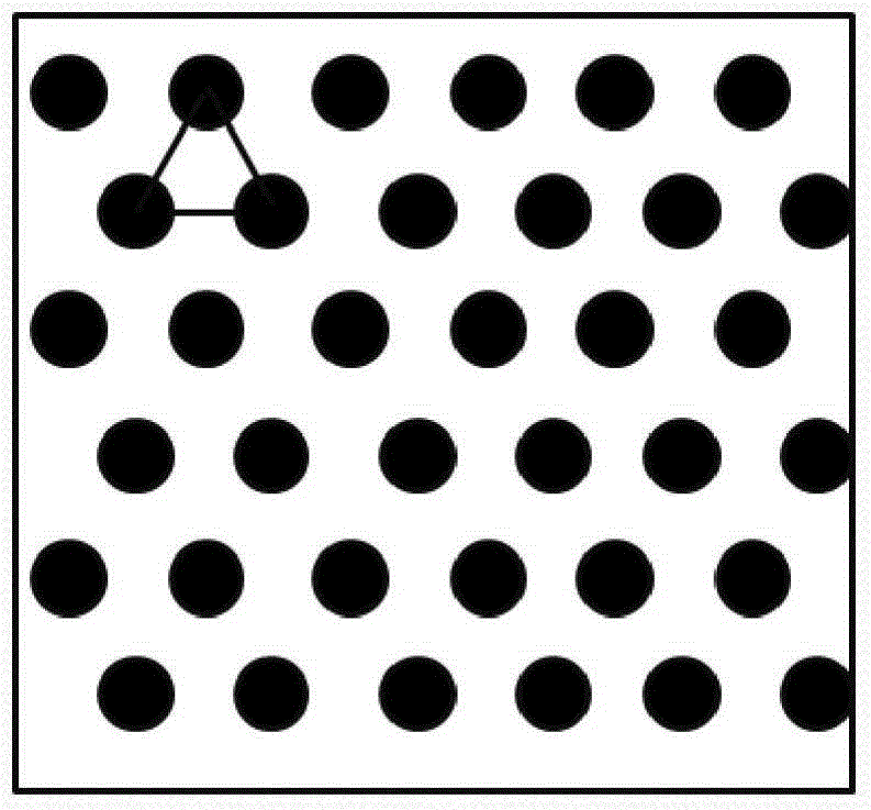
[0023] Such as image 3 As shown, the reflective photonic crystal, that is, photonic crystal-103, has an air-hole structure in a periodic triangular arrangement structure, its lattice period is 300nm, and the etching depth is 200nm.

[0024] Such as Figure 4 , Figure 5 , Figure 6 As shown, the defect-type photonic crystal, that is, photonic crystal 2 106, has a structure of air holes or dielectric columns, which is one of periodic square, rhombus or hexagonal arrangements, and its lattice period ranges from 200 to 800nm, and the etching depth is 40-20...


PUM


Abstract

Provided is a quantum dot LED with a dual photonic crystal structure, successively comprising a substrate 101, a hole injection layer 102, a reflection type photonic crystal 103 (i.e., a first photonic crystal) arranged on the hole injection layer 102, a hole transmission layer 104, a quantum dot active region 105, a deficit type photonic crystal 106 (i.e., a second photonic crystal) arranged on an electronic transmission layer 107, the electronic transmission layer 107, and an electron injection layer 108 from bottom to top. The beneficial effects are that the quantum dot LED can substantially increase LED light extraction efficiency, and finally favor the increase of LED luminescence power and brightness.

Description

technical field [0001] The invention relates to the field of semiconductor optoelectronic devices, in particular to a quantum dot light-emitting diode with a two-photon crystal structure. Background technique [0002] Quantum dots have a quantum size confinement effect. By changing the size of quantum dots, different wavelengths of light can be realized. Quantum dot-based light-emitting diode devices have the advantages of full color, high purity, good monochromaticity, adjustable color, and large-scale preparation. [0003] Quantum dot light-emitting diode LEDs prepared in the prior art usually adopt a sandwich structure, such as figure 2 shown. That is, the thin film containing quantum dots is arranged between the p-type and n-type semiconductor thin film materials, but the quantum dot LED with this structure is not as high as the common multi-quantum well LED. Because the luminous efficiency is determined by both the internal quantum efficiency and the light extraction...

Claims


Application Information

Patent Timeline
Patent Type & Authority Applications(China)
IPC IPC(8): H01L33/16H01L33/06
CPCH01L33/06H01L33/16
Inventor 张雄吴自力崔一平
Owner SOUTHEAST UNIV
Why Eureka
Try Eureka