
Energetic semiconductor bridge and preparation method thereof

A technology of semiconductors and oxides, applied in the field of semiconductor bridges, can solve the problems of difficult preparation of reactive semiconductor bridges, high production costs, complex processes, etc., and achieve the effects of shortening the diffusion and mass transfer distance, convenient equipment, and accelerating the reaction rate

Inactive Publication Date: 2015-10-14
NANJING UNIV OF SCI & TECH
View PDF4 Cites 16 Cited by
  • Summary
  • Abstract
  • Description
  • Claims
  • Application Information

AI Technical Summary

Problems solved by technology

[0011] The multi-layer metal semiconductor composite bridge in patent 3 has a more complex structure than polysilicon and single-layer metal semiconductor composite bridges, and the production cost is also higher
[0012] The preparation of the reactive semiconductor bridge in patent 4 is difficult, the process is complicated, and the cost is high

Method used


Image

  • Energetic semiconductor bridge and preparation method thereof
  • Energetic semiconductor bridge and preparation method thereof
  • Energetic semiconductor bridge and preparation method thereof

Examples


preparation example Construction

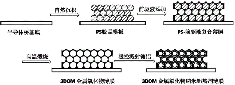
[0039] combine figure 2 , the preparation method of the energetic semiconductor bridge of the present invention comprises the following steps:

[0040] Step 1, preparing PS microspheres, the particle size of the PS microspheres is 200-800nm, dispersed in water to form a PS microsphere emulsion, and the concentration of the PS microsphere emulsion is 2-10wt%;

[0041] Step 2, preparing metal oxide precursor liquid; including the following two metal oxide precursor liquids, respectively as follows:

[0042] (a) the preparation of metal oxide precursor solution, wherein the metal oxide is Mn 2 o 3 , the configuration process of the precursor solution is as follows: Mn(Ac) 2 4H 2 O was added to the mixed solvent of methanol and ethylene glycol and stirred until Mn(Ac) 2 4H 2 O is completely dissolved, and PVP (10000) is added to adjust the viscosity of the precursor solution; the molar ratio of methanol and ethylene glycol is 3:1; Mn(Ac) 2 4H 2 The mass of O added is 0.3-...

Embodiment 1

[0050] Step 1: Prepare PS microspheres with smooth surface, monodisperse and particle size of 200nm in the laboratory, and disperse them in water to form PS microsphere emulsion with a concentration of 5wt%.

[0051] Step 2: Weigh 7.35g Mn(Ac) 2 4H 2 O was added to 20mL of methanol: ethylene glycol molar ratio was 3:1 mixed solvent and stirred for 2h until Mn(Ac) 2 4H 2 O is completely dissolved for later use. Then weigh 1.0g PVP (10000) and add it to the solution, stir for 12 hours to obtain a certain viscosity of Mn 2 o 3 precursor solution.

[0052] Step 3: Drop 0.05ml of PS microsphere emulsion on the semiconductor bridge substrate, let it dry naturally, then dry it in a vacuum oven at 40°C for 1 hour, and cool it down to room temperature. Three-dimensional long-range ordered PS microsphere colloidal thin films were vertically deposited on semiconductor bridge substrates.

[0053] Step 4: Drop 0.10ml of Mn on the PS microsphere colloidal crystal film obtained in ste...

Embodiment 2

[0061] Step 1: Prepare PS microspheres with smooth surface, monodisperse and particle size of 380nm in the laboratory, and disperse them in water to form PS microsphere emulsion with a concentration of 5wt%.

[0062] Step 2: Weigh 7.35g Mn(Ac) 2 4H 2 O was added to 20mL of methanol: ethylene glycol molar ratio was 3:1 mixed solvent and stirred for 2h until Mn(Ac) 2 4H 2 O is completely dissolved for later use. Then weigh 1.0g PVP (10000) and add it to the solution, stir for 12 hours to obtain a certain viscosity of Mn 2 o 3 precursor solution.

[0063] Step 3: Drop 0.05ml of PS microsphere emulsion on the semiconductor bridge substrate, let it dry naturally, then dry it in a vacuum oven at 40°C for 1 hour, and cool it down to room temperature. Three-dimensional long-range ordered PS microsphere colloidal thin films were vertically deposited on semiconductor bridge substrates.

[0064] Step 4: Drop 0.10ml of Mn on the PS microsphere colloidal crystal film obtained in ste...


PUM


Abstract

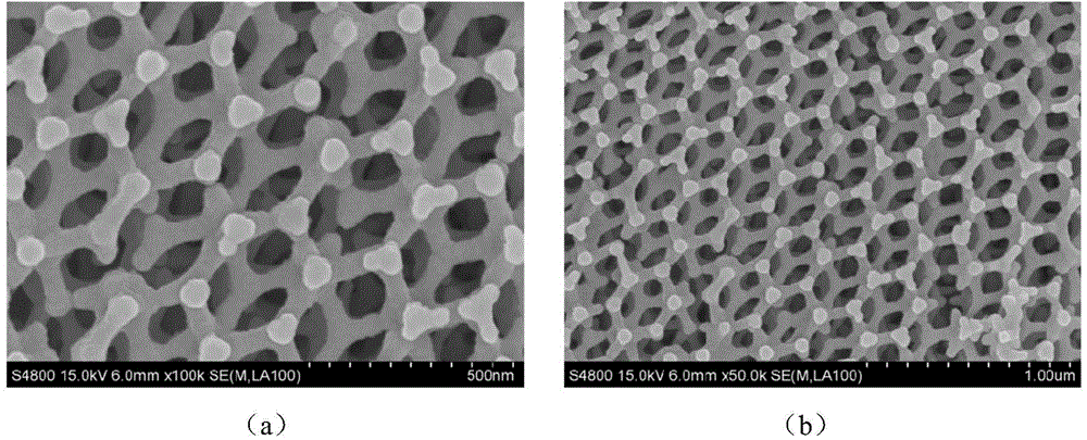
The invention discloses an energetic semiconductor bridge and a preparation method thereof. The energetic semiconductor bridge comprises a semiconductor bridge substrate and a 3DOM (Three-Dimensionally Ordered Macroporous) metal oxide nano-thermite film prepared on the semiconductor bridge substrate. The preparation method comprises the steps that a PS microsphere emulsion is prepared; metal oxide precursor liquid is prepared; the PS microsphere emulsion is dropwise added onto the semiconductor bridge substrate and dried; PS microspheres deposits naturally to form a colloidal crystal template; the metal oxide precursor liquid is dropwise added onto the colloidal crystal template, permeates through the colloidal crystal template, and is dried to form a PS microsphere / precursor liquid composite film; the PS microsphere / precursor liquid composite film is put in a muffle furnace to be calcined for PS colloidal crystal template removal, and a 3DOM metal oxide skeleton is produced; the 3DOM metal oxide skeleton on the semiconductor bridge substrate is aluminized with the adoption of magnetron sputtering; and the semiconductor bridge containing the 3DOM metal oxide nano-thermite film is obtained. The energetic semiconductor bridge is mild in preparation condition, and the prepared energetic semiconductor bridge has the advantages of high ignition quantity and long ignition time.

Description

technical field [0001] The invention belongs to the technical field of semiconductor bridges, in particular to an energetic semiconductor bridge and a preparation method thereof. Background technique [0002] Pyrotechnics are the first functional components of weapons and equipment. With the development of high-tech engineering technology, the requirements for the safety and reliability of pyrotechnics are getting higher and higher, and semiconductor bridge pyrotechnics came into being. The semiconductor bridge pyrotechnic product was born in 1968. It has the advantages of high instantaneity, high safety, high reliability, low ignition energy and can be combined with digital logic circuits. At present, the ignition, attitude control, ballistic correction, unlocking and separation, and safety insurance of digitized and intelligent weapons and ammunition are all inseparable from micro-ignition and detonation sequence modules (chips). In addition, the civilian fields such as a...

Claims


Application Information

Patent Timeline
Patent Type & Authority Applications(China)
IPC IPC(8): F42B3/13B82Y30/00B82Y40/00
Inventor 张文超俞春培秦志春焦阳叶家海田桂蓉张学舜
Owner NANJING UNIV OF SCI & TECH
Learn More