A terahertz wave time-domain spectrum system based on an ultra-wideband chip

An ultra-wideband, chip technology, applied in the field of terahertz wave detection, to achieve the effect of simple structure and easy realization

Active Publication Date: 2018-11-20
UNIV OF SHANGHAI FOR SCI & TECH
View PDF8 Cites 0 Cited by
  • Summary
  • Abstract
  • Description
  • Claims
  • Application Information

AI Technical Summary

Problems solved by technology

Although the waveguide filter and high-fidelity structure of waveguide-coupled surface plasmons is a very mature technology in the visible light band, the corresponding systems working in the terahertz band are rarely reported, especially the high-fidelity and double-layer Ultra-wideband filters with waveguide structures have not been involved

Method used


Image

  • A terahertz wave time-domain spectrum system based on an ultra-wideband chip
  • A terahertz wave time-domain spectrum system based on an ultra-wideband chip
  • A terahertz wave time-domain spectrum system based on an ultra-wideband chip

Examples


Embodiment Construction

[0019] The specific implementation manners of the present invention will be described below in conjunction with the accompanying drawings.

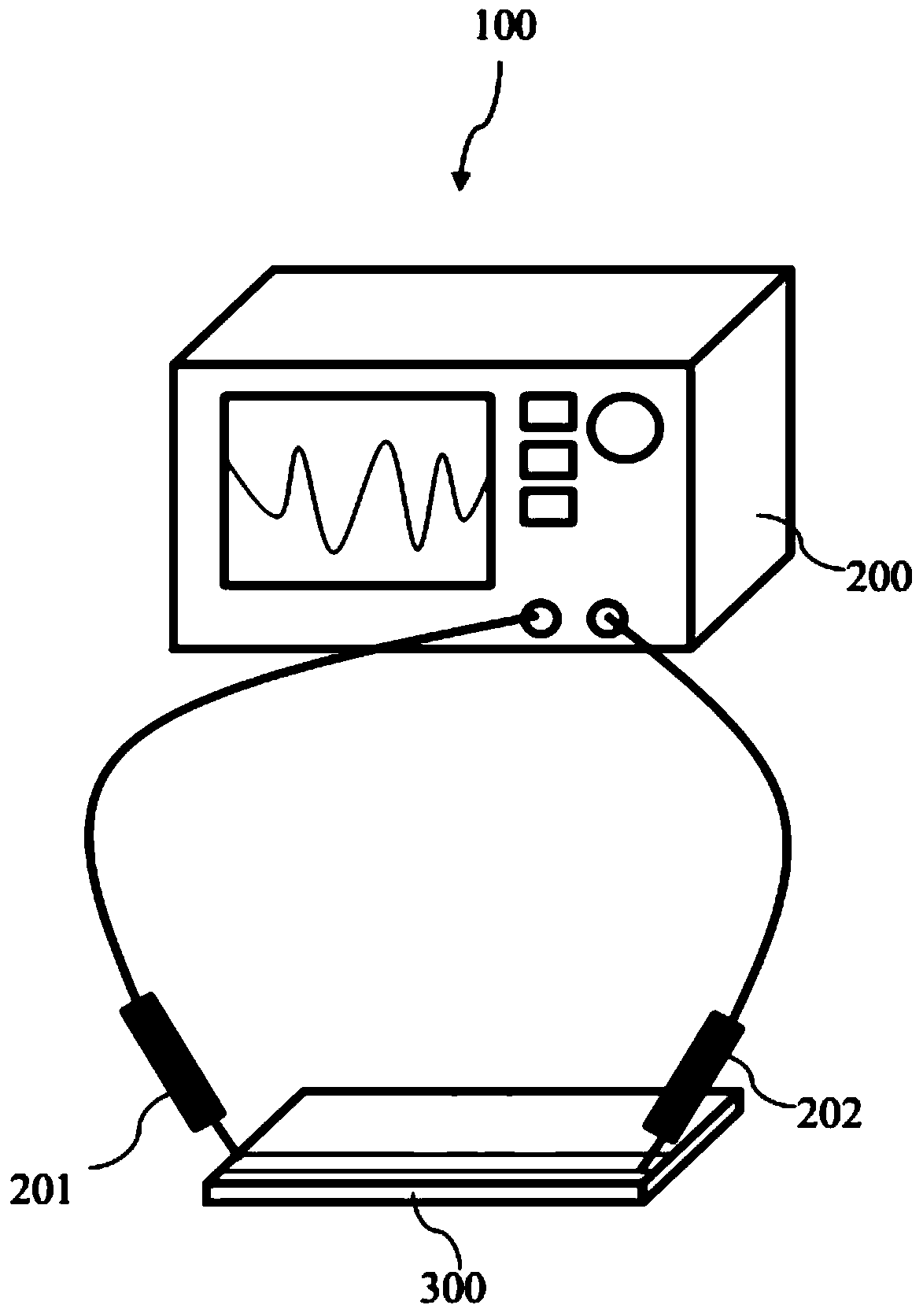
[0020] figure 1 It is a schematic structural diagram of the ultra-wideband chip-based terahertz wave time-domain spectrum system of this embodiment.

[0021] Such as figure 1 As shown, the ultra-wideband chip-based terahertz wave time-domain spectrum system 100 includes a vector network analyzer 200 and an ultra-wideband chip 300 . The vector network analyzer 200 is connected to the energy transmission port of the ultra-wideband chip 300 through the probe 201 and the probe 202 respectively, and is used for transmitting and detecting terahertz wave signals.

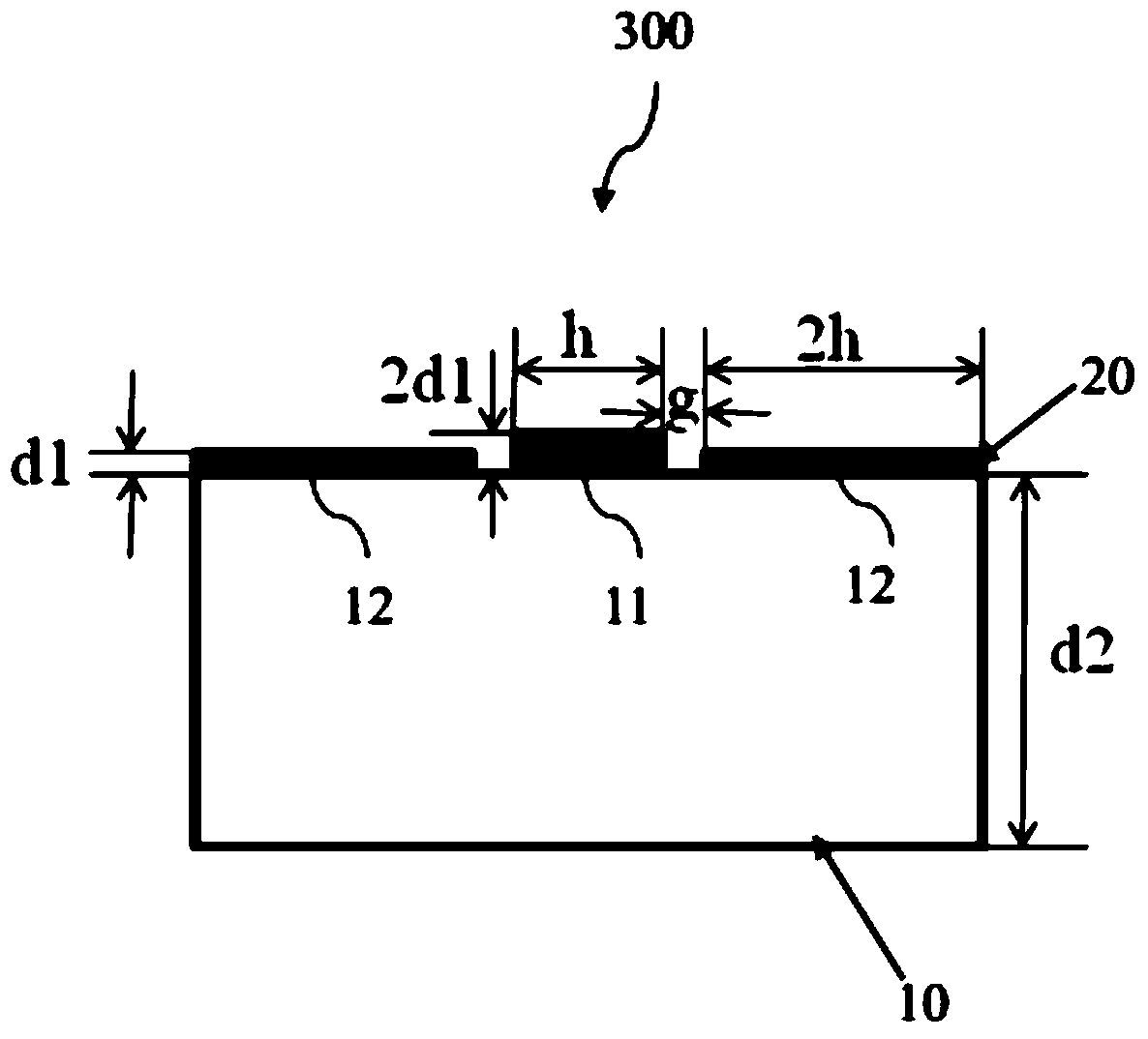
[0022] figure 2 It is a structural schematic diagram of the ultra-wideband chip of this embodiment.

[0023] Such as figure 2 As shown, the ultra-wideband chip 300 is composed of a substrate 10 and a metal layer 20 . The metal layer 20 is attached on the substrate 10 by photol...


PUM


Abstract

The invention provides a terahertz time-domain spectrum system based on an ultra-wideband chip. The system comprises a substrate and a metal layer. The metal layer is used for acquiring and conducting terahertz, and comprises a signal acquisition unit, a first mode switching part, a conducting part, a second mode switching part and a signal output part. The first mode switching part, the conducting part and the second mode switching part are of double waveguide structure. The signal acquisition part is used for acquiring the terahertz from a host device, and transmitting the terahertz to the first mode switching part for mode switching. The terahertz is changed into a surface wave. The surface wave is transmitted in the double waveguide of the conducting part, so as to form an energy band gap for filtering. The second mode switching part carries out mode switching again. The signal output part transmits the wave to a vector network analyzer for data analysis, so as to acquire the width of a band-pass band.

Description

technical field [0001] The invention belongs to the field of terahertz wave detection, and in particular relates to a terahertz wave time-domain spectrum system based on an ultra-wideband chip. Background technique [0002] With the development of modern wireless communication technology, ultra-wideband technology has received widespread attention in recent years. Modern communication products are widely used, and the frequency bands used by each product are different. To use these frequency bands simultaneously requires a wide-band transceiver system. [0003] Coplanar waveguide is an important means to realize broadband technology. It is actually surface plasmon resonance, which is a kind of charge density oscillation eigenmode existing at the interface of metal and dielectric, which can be excited by incident light through prism coupling, grating coupling or waveguide coupling. The ultra-wideband filter based on the double-layer structure of the coplanar waveguide reali...

Claims


Application Information

Patent Timeline
Patent Type & Authority Patents(China)
IPC IPC(8): H01P1/203
Inventor 陈麟朱亦鸣汪丹妮魏玉明韦鹏蔡斌臧小飞庄松林
Owner UNIV OF SHANGHAI FOR SCI & TECH
Why Eureka
Try Eureka