Measuring device for Raman scattered spectrum and Raman scattering spectrometer

A technology of Raman scattering spectroscopy and Raman scattering, which is applied in the field of Raman scattering spectrometers and Raman scattering spectroscopy measurement devices, can solve the problems of limited elimination of short-lived fluorescent signals, narrow spectral response range, and insufficient time resolution. , to improve photon counting efficiency and time resolution, reduce fluorescence interference, and improve signal-to-noise ratio

Active Publication Date: 2015-11-04
BEIJING NORMAL UNIVERSITY
View PDF4 Cites 16 Cited by
  • Summary
  • Abstract
  • Description
  • Claims
  • Application Information

AI Technical Summary

Problems solved by technology

This technology based on gated ICCD detector is simpler than Kerr optical switch technology, and its time resolution is generally at the nanosecond level, but the inherent excess noise of ICCD limits its maximum signal-to-noise ratio, its quantum efficiency is low, and its sp

Method used


Image

  • Measuring device for Raman scattered spectrum and Raman scattering spectrometer

Examples


Embodiment Construction

[0019] In order to make the object, technical solution and advantages of the present invention clearer, the present invention will be described in further detail below in conjunction with the embodiments and accompanying drawings. Here, the exemplary embodiments and descriptions of the present invention are used to explain the present invention, but not to limit the present invention.

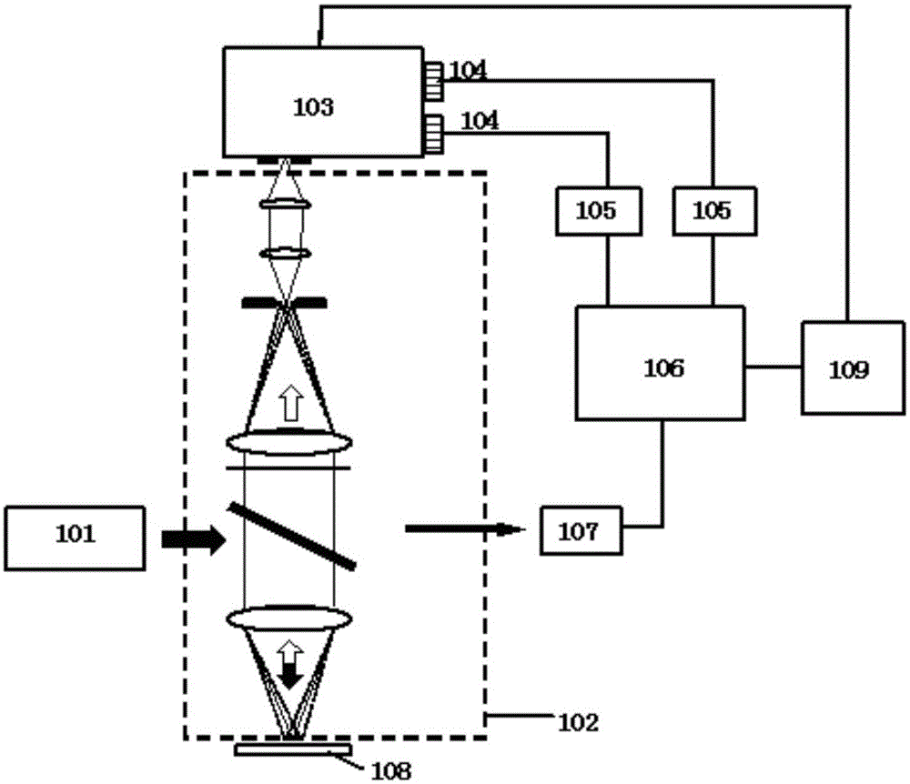
[0020] In an embodiment of the present invention, a measurement device for Raman scattering spectrum is provided, such as figure 1 As shown, the device includes: a pulsed laser 101, a Raman scattering optical path 102 (such as figure 1 shown in the dotted line box), grating monochromator 103, signal photodetector 104, reference photodetector 107 and spectrum generation device, wherein,

[0021] The pulsed laser 101 is arranged on one side of the Raman scattering light path and is used to emit laser light (such as figure 1 Indicated by the black arrow in ) to excite the sample 108 to generate ...


PUM


Abstract

The invention provides a measuring device for a Raman scattered spectrum and a Raman scattering spectrometer. A path of laser emitted from a pulse laser excites a sample and a Raman scattered light signal is generated; a Raman scattered light path transmits the Raman scattered light signal to a grating monochromator; the grating monochromator transmits the Raman scattered light signal to a signal light detector; the pulse laser emits another path of laser to a reference light detector, and the reference light detector outputs a timing beginning signal of the Raman scattering event according to the laser; the signal light detector carries out precise counting measurement of photons comprised by each light pulse of the Raman scattered light signal in a preset time period with the timing beginning signal as a start, and the light detector is a silicon photoelectric multiplier; a spectrum generation device generates a Raman scattered spectrum according to the photon number of all the light pulses of the Raman scattered light signal. The time resolution is raised, the photon counting efficiency is raised and the signal to noise ratio and the detection speed are raised.

Description

technical field [0001] The invention relates to the technical field of material detection, in particular to a Raman scattering spectrum measuring device and a Raman scattering spectrometer. Background technique [0002] In recent years, a silicon photomultiplier (also known as silicon photomultiplier tube, SiPM or MPPC) derived from the research of nuclear physics semiconductor detectors has received extensive attention from researchers [see D. Renker, "Geiger-mode avalanche photodiodes, history, properties and problems”, Nuclear Instruments and Methods in Physics Research A 567(2006) 48–56; Elena V. Popova et al., “Silicon Photomultiplier (Deformation) and Silicon Photomultiplier Unit”, Application No. : 200580019248.1]. SiPM consists of hundreds to thousands of avalanche photodiode (APD) units with a diameter of tens to tens of microns integrated on the same single crystal silicon wafer. All APD units are output in parallel and share one load. Each APD unit works above t...

Claims


Application Information

Patent Timeline
IPC IPC(8): G01J3/44
Inventor 韩德俊王慎远苗泉龙
Owner BEIJING NORMAL UNIVERSITY
Why Eureka
Try Eureka