

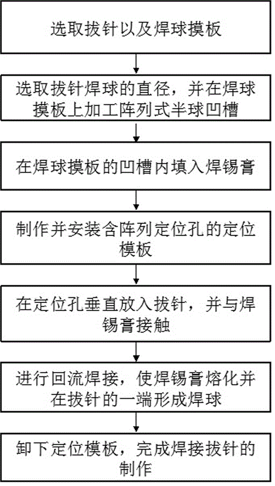
Manufacturing method of welding pull pins
A production method and solder ball technology, applied in the direction of welding equipment, manufacturing tools, auxiliary devices, etc., can solve the problems of cracking and easy breakage of PCB pads, and achieve the effect of pertinence, strong controllability and simple operation.
- Summary
- Abstract
- Description
- Claims
- Application Information
AI Technical Summary
Problems solved by technology
Method used
Image

Examples
Embodiment
[0027] Such as figure 1 Shown, a kind of manufacturing method of welding pin, comprises the steps:
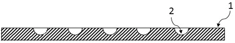
[0028] 1) Select pin 7. In this embodiment, a copper-plated pin with a diameter of 0.45mm is used, and solder ball template 1 is selected. The template material in this embodiment is bakelite, such as figure 2 shown;
[0029] 2) According to the pin diameter of 0.45 mm, the diameter of the solder ball 8 required for the pin 7 is selected to be 0.6 mm, and the arrayed hemispherical groove 2 corresponding to the diameter of the solder ball 8 is set on the solder ball template 1, as shown in figure 2 As shown, the radius of groove 2 is 1mm;
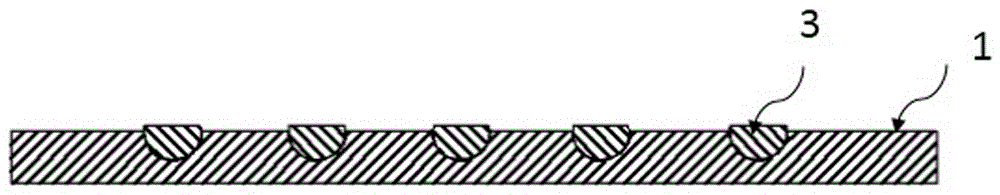
[0030] 3) Fill the solder paste 3 in the groove 2 of the solder ball template 1, such as image 3 shown;
[0031] 4) Make a positioning template 4 containing an array of positioning holes 6, and fix the positioning template 4 directly above the solder ball template 1 through the pillar 5, wherein the positions of the array positioning h...
PUM
| Property | Measurement | Unit |
|---|---|---|
| radius | aaaaa | aaaaa |
Abstract
Description
Claims
Application Information