A method of using pci master mode to realize data interaction between boards

A technology of data interaction and main mode, applied in the direction of electrical digital data processing, hardware monitoring, instruments, etc., can solve the problems of large data delay and instability, and achieve the effects of speed and stability, flexible use, and convenient expansion

Active Publication Date: 2017-11-03
HARBIN INST OF TECH
View PDF2 Cites 0 Cited by
  • Summary
  • Abstract
  • Description
  • Claims
  • Application Information

AI Technical Summary

Problems solved by technology

[0006] The purpose of the present invention is to provide a method of utilizing the PCI main mode to realize data interaction between boards, reduce the data interaction or access delay between different boards on the same PCI bus through the PCI main mode, and solve the problems caused by host computer software synchronization or framing The resulting data delay is large, unstable and other problems

Method used


Image

  • A method of using pci master mode to realize data interaction between boards
  • A method of using pci master mode to realize data interaction between boards
  • A method of using pci master mode to realize data interaction between boards

Examples


specific Embodiment approach 1

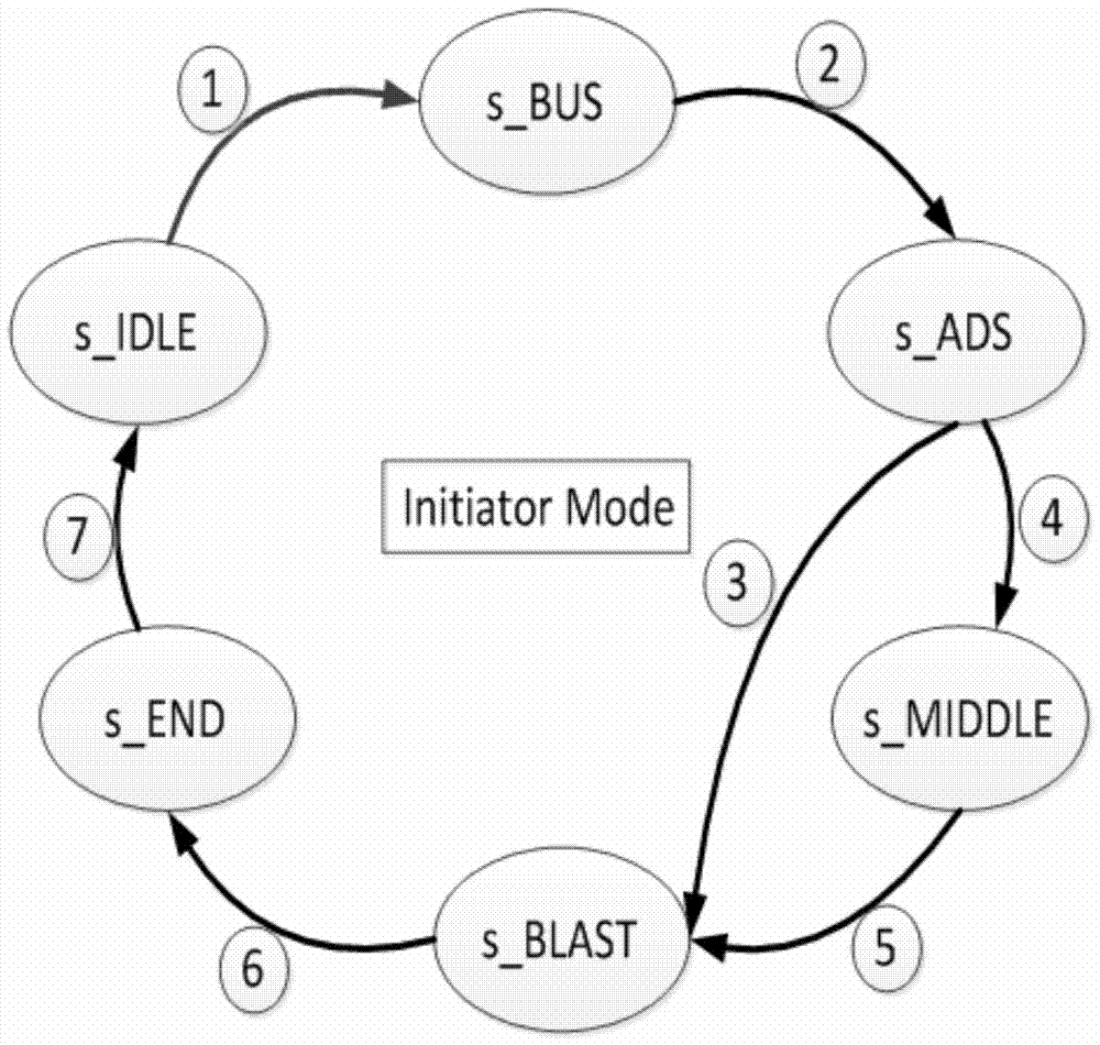
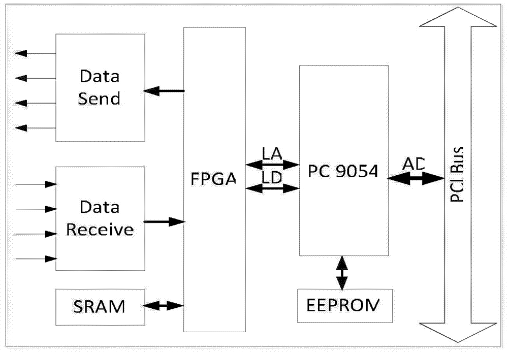
[0045] Specific implementation mode one: as Figure 1~5 As shown, the actual process of implementing the method for data interaction between boards in the PCI master mode is described in this embodiment:

[0046] The PCI main mode refers to that the PCI bus bridge chip PCI9054 can actively apply for bus use and control rights as the initiator of PCI bus end data transmission;

[0047] The implementation of the method needs to involve two boards, namely a master mode board and a slave mode board; the board that actively initiates data transmission is called a master mode board, and the board that passively cooperates to complete data transmission is called a slave mode Board: The main mode board based on the PCI bridge chip design completes the PCI main mode data transmission through the internal program of the hardware board or logic control bridge chip, and realizes the access to the board on the PCI bus;

[0048] The realization process of described method is:

[0049] Ste...

specific Embodiment approach 2

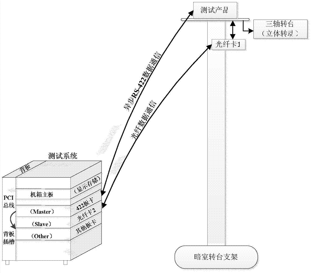
[0078] Embodiment 2: This embodiment is the application of the method described in Embodiment 1. The method is applied to the darkroom test of microwave radar products. The implementation process is as follows:

[0079] The hardware boards based on the darkroom test process of microwave radar products include: master mode board and slave mode board (in the same test equipment), darkroom turntable, test products and signal sources placed on the darkroom turntable, etc.; , the main mode board and the test product have been communicating regularly, and the communication data includes the distance, azimuth, pitch and angular velocity information measured by the microwave radar; The time delay transmits data, and the darkroom turntable shares its own angle information with the slave mode board in real time (almost no delay);

[0080] First of all, after sending a frame of data each time, the master mode board starts master mode data reading, directly reads the specified offset addr...


PUM


Abstract

A method for realizing data interaction between boards by using the PCI master mode. The invention can realize data access between different boards on the same bus or read data from dedicated memory boards on the bus, and can further solve problems in some test occasions. , Due to the synchronization or framing of the upper computer software, the data delay is large and unstable. The realization of the main mode function mainly lies in the hardware design of the main mode board, the related logic design of the local bus terminal and the configuration of the bridge chip PCI9054. Using the combination of FPGA and PCI9054, the hardware and logic design of the PCI interface at the local bus end is completed, and the data transmission function in the main mode can be realized more perfectly. It can be applied in the fields of communication, measurement and control, etc., and the real-time requirements of data interaction between boards in the system are high. Utilizing the advantages of the PCI bus, it realizes the design of the PCI main mode, improves the real-time performance of data interaction between test boards, has stable performance, and has good scalability.

Description

technical field [0001] The invention relates to a method for realizing data interaction between different test boards on the same PCI bus by using a PCI main mode, and relates to the fields of communication and measurement and control. Background technique [0002] In the later stages of testing many aerospace products, it is necessary to simulate the actual environment for testing. The microwave anechoic chamber can provide a pure electromagnetic environment and a turntable, which not only meets the requirements of all-round testing of products, but also reduces the harm of microwaves to human body through its shielding effect. However, some product tests require good real-time data interaction and a small delay between data. For example, it may be necessary to synchronize product test data and turntable information into frames, etc. It is of great significance to study a hardware testing scheme with good real-time data interaction and stable performance. [0003] The con...

Claims


Application Information

Patent Timeline
Patent Type & Authority Patents(China)
IPC IPC(8): G06F11/34G06F13/362
Inventor 付宁刘通徐东东乔立岩
Owner HARBIN INST OF TECH
Why Eureka
Try Eureka