Manufacturing method of tft substrate and structure of tft substrate

A manufacturing method and substrate technology, applied in semiconductor/solid-state device manufacturing, electrical components, electrical solid-state devices, etc., can solve problems such as difficulty in machine debugging, long time consumption, and strict requirements on mask accuracy, and achieve low production costs, Reduce production costs and make simple effects

Active Publication Date: 2018-03-30
TCL CHINA STAR OPTOELECTRONICS TECH CO LTD
View PDF5 Cites 0 Cited by
  • Summary
  • Abstract
  • Description
  • Claims
  • Application Information

AI Technical Summary

Problems solved by technology

In the ion implantation process, it is most common to use an ion implanter to achieve ion implantation. For example, the channel region, N-type heavily doped region, N-type lightly doped region, and P-type doped region are generally implanted by ion implanters. Ion implantation, and each ion implantation process needs to be completed with a photomask, and the ion implantation process has strict requirements on the accuracy of the photomask, and there are problems such as difficulty in machine debugging and long time consumption

Method used


Image

  • Manufacturing method of tft substrate and structure of tft substrate
  • Manufacturing method of tft substrate and structure of tft substrate
  • Manufacturing method of tft substrate and structure of tft substrate

Examples


Embodiment Construction

[0035] In order to further illustrate the technical means adopted by the present invention and its effects, the following describes in detail in conjunction with preferred embodiments of the present invention and accompanying drawings.

[0036] see figure 1 , the present invention at first provides a kind of manufacture method of TFT substrate, comprises the following steps:

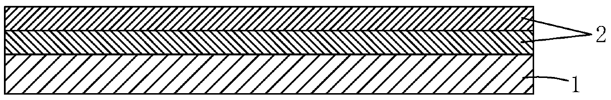
[0037] Step 1, such as figure 2 As shown, a substrate 1 is provided on which a buffer layer 2 is deposited.

[0038] Specifically, the substrate 1 may be a glass substrate or a plastic substrate.

[0039] Specifically, the buffer layer 2 may be a silicon oxide (SiOx) layer, a silicon nitride (SiNx) layer, or a composite layer of a silicon oxide layer and a silicon nitride layer. In this embodiment, the buffer layer 2 is a composite layer of a silicon oxide layer and a silicon nitride layer.

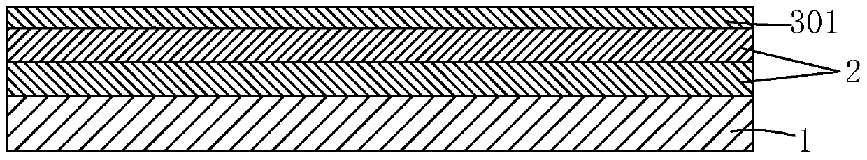
[0040] Step 2, such as image 3 As shown, an amorphous silicon (a-Si) thin film 301 is deposited on the buf...


PUM


Abstract

The invention provides a structure and preparation method of a TFT substrate. According to the preparation method, a multi-step filming manner is employed in the process of preparing an amorphous silicon layer, boron ion implantation is carried out on the amorphous silicon layer via CVD surface processing by utilizing a boron hydride gas after each step of filming, and the amorphous silicon layer doped with boron ions is obtained. According to the structure of the TFT substrate, implantation of boron ions is completed during amorphous silicon filming of a channel region, it is not required to doping the channel region independently after the channel region is formed, the process is effectively simplified, and the production cost is reduced.

Description

technical field [0001] The invention relates to the field of display technology, in particular to a manufacturing method of a TFT substrate and a structure of the TFT substrate. Background technique [0002] In the field of display technology, flat panel displays such as Liquid Crystal Display (LCD) and Organic Light Emitting Diode (OLED) have gradually replaced CRT displays. [0003] Generally, a liquid crystal display device includes a housing, a liquid crystal panel disposed in the housing, and a backlight module disposed in the housing. Among them, the structure of the liquid crystal panel is mainly composed of a thin film transistor array substrate (Thin FilmTransistor Array Substrate, TFT Array Substrate), a color filter substrate (ColorFilter, CF), and a liquid crystal layer (Liquid Crystal Layer) arranged between the two substrates. ), its working principle is to control the rotation of the liquid crystal molecules in the liquid crystal layer by applying a driving v...

Claims


Application Information

Patent Timeline
Patent Type & Authority Patents(China)
IPC IPC(8): H01L21/77H01L27/12H01L21/22
CPCH01L21/2205H01L21/77
Inventor 张良芬
Owner TCL CHINA STAR OPTOELECTRONICS TECH CO LTD
Why Eureka
Try Eureka