

FinFET manufacturing method
A manufacturing method and technology of fins, applied in semiconductor/solid-state device manufacturing, semiconductor devices, electrical components, etc., can solve the problems of increased impurity concentration and distribution widening, and achieve the effect of improving device performance and optimizing process
- Summary
- Abstract
- Description
- Claims
- Application Information
AI Technical Summary
Problems solved by technology
Method used
Image

Examples
Embodiment Construction
[0019] In view of the above problems, the present invention provides a FinFET manufacturing method, which effectively optimizes the distribution of PTSL so that it can be well concentrated in the place where the through current is generated without affecting other performances of the device. Specifically, the method includes:
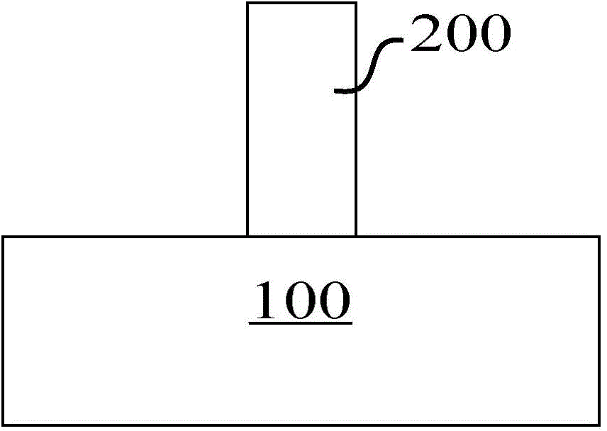
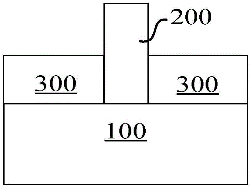
[0020] a. providing a substrate 100, and forming fins 200 on the substrate;
[0021] b. forming isolation layers 300 on the substrates on both sides of the fin 200;
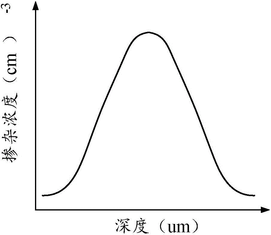
[0022] c. forming a punch-through barrier layer 310 in part of the fins covered by the isolation layer 300, so that the position of the impurity concentration peak in the punch-through barrier layer is lower than the surface of the isolation layer;
[0023] d. Etching the isolation layer 300 so that its surface is flush with the position where the impurity concentration peak of the punch-through barrier layer 310 is located;
[0024] e. Forming source and drain regions at both ends of th...
PUM
| Property | Measurement | Unit |
|---|---|---|
| Thickness | aaaaa | aaaaa |
Abstract
Description
Claims
Application Information