A kind of electroluminescence display device and its preparation method

A display device and electroluminescence technology, which is applied in the direction of image/graphic display tubes, electrical components, electrode devices and related components, etc., can solve the problems of difficulty in supplying electrons in the conduction band of materials, complicated preparation process of emission cathodes, and limitations in emission performance. , to achieve the effect of reducing device cost, simple structure and improving resolution

Active Publication Date: 2018-01-02
SHAANXI UNIV OF SCI & TECH
View PDF6 Cites 0 Cited by
  • Summary
  • Abstract
  • Description
  • Claims
  • Application Information

AI Technical Summary

Problems solved by technology

At present, the shapes of field emission cathodes include tapered and flat film types. The preparation process of tapered field emission cathodes is complex, difficult, and costly, and it is not easy to make large-area display devices; the flat film type generally adopts diamond film or diamond-like type. However, diamond is a material with negative electron affinity. Negative electron affinity makes electrons migrate into the material, making it difficult to replenish electrons in the conduction band of the material. In addition, diamond has a high resistance, resulting in limited field emission performance.

Method used


Image

  • A kind of electroluminescence display device and its preparation method
  • A kind of electroluminescence display device and its preparation method
  • A kind of electroluminescence display device and its preparation method

Examples


Embodiment Construction

[0033] The present invention will be described in detail below in conjunction with the accompanying drawings and embodiments.

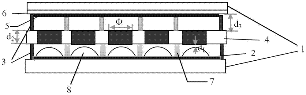
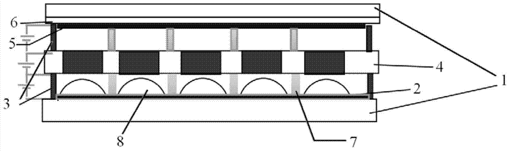
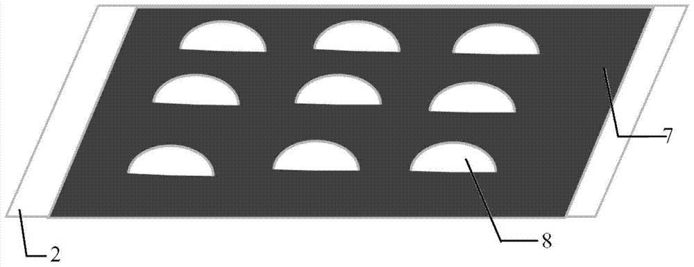
[0034] see figure 1 , figure 2 as well as image 3 , the electroluminescent display device of the present invention comprises two substrates 1, a cathode 2, a sealant 3, a microchannel plate 4 (the upper and lower surfaces are respectively attached with an upper electrode 9 and a lower electrode 10), an anode 5, a fluorescent powder Layer 6, spacers 7 and field electron emitters 8 (for emitting electrons).

[0035] The cathode 2 is arranged on one of the substrates, and a plurality of field electron emitters 8 are arranged at intervals in a matrix on the cathode 2, and the phosphor layer 6 is arranged on the other substrate, and the anode 5 is arranged on the phosphor layer 6, and the field electron A microchannel plate 4 is arranged between the emitter 8 and the anode 5, and the spacer column 7 covers the cathode area except the edge of the catho...


PUM


Abstract

The invention provides an electroluminescent display device and a preparation method thereof, comprising a substrate, a cathode, an anode, a phosphor layer, an electron emitter and an isolation column, and the isolation column is formed for each field electron emitter from the cathode through a microchannel plate The upper corresponding area or the mutually isolated electron movement channel corresponding to the microchannel to the anode, the microchannel plate can effectively play the effect of electron multiplication, and the isolation column can play the role of controlling thickness, dividing pixels and insulating; The electroluminescent display device structure has a wide selection of device materials and a simple preparation process, and can improve device resolution, gray scale, contrast and other performances and reduce device cost.

Description

technical field [0001] The invention belongs to the display field, and in particular relates to an electroluminescence display device structure. Background technique [0002] Field electron emission refers to the emission that applies a strong electric field on the surface of an object to weaken the binding energy that prevents electrons from escaping from the object, and uses the tunneling effect to make it escape from the object. The field emission current density is closely related to the field strength of the applied electric field and the work function of the emitter. At present, the shapes of field emission cathodes include tapered and flat film types. The preparation process of tapered field emission cathodes is complex, difficult, and costly, and it is not easy to make large-area display devices; the flat film type generally adopts diamond film or diamond-like type. However, diamond is a material with negative electron affinity. Negative electron affinity allows ele...

Claims


Application Information

Patent Timeline
Patent Type & Authority Patents(China)
IPC IPC(8): H01J31/12H01J29/04H01J29/46
Inventor 张麦丽牟强
Owner SHAANXI UNIV OF SCI & TECH
Why Eureka
Try Eureka