Enhanced HEMT of integrated SBD

An enhanced and U-shaped technology, applied in semiconductor devices, electrical components, circuits, etc., can solve the problems of difficult balance of performance, single device function, and slow development of simple integrated devices, and achieve high blocking voltage, protection devices and The effect of the circuit

Active Publication Date: 2015-12-02
UNIV OF ELECTRONICS SCI & TECH OF CHINA
View PDF6 Cites 13 Cited by
  • Summary
  • Abstract
  • Description
  • Claims
  • Application Information

AI Technical Summary

Problems solved by technology

[0005] In addition, there are still many problems hindering the development of GaN devices and circuits, such as the difficulty of realizing enhanced devices with better performance, the slow development of simple integrated devices, the single function of devices and their different performances but difficult to balance, etc.

Method used


Image

  • Enhanced HEMT of integrated SBD
  • Enhanced HEMT of integrated SBD
  • Enhanced HEMT of integrated SBD

Examples


Embodiment Construction

[0035] Below in conjunction with accompanying drawing, describe technical scheme of the present invention in detail:

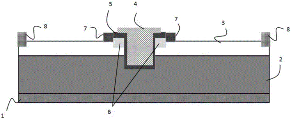
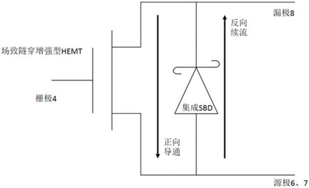
[0036] According to the principle that the MOS structure forms a strong inversion layer on the surface of the semiconductor layer and modulates the thickness of the Schottky contact barrier under the gate voltage modulation to make the source electrons easier to tunnel, the groove gate is formed by using a self-alignment process. As well as different work function metal deposition techniques, an enhanced AlGaN / GaN HEMT device with integrated Schottky barrier diode (SBD) is realized.

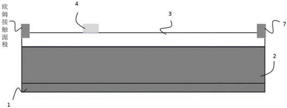
[0037]A kind of enhanced HEMT integrated SBD of the present invention, such as figure 1 As shown, it includes a substrate 1, a buffer layer 2 positioned on the upper surface of the substrate, and a barrier layer 3 positioned on the upper surface of the buffer layer 2, and the buffer layer 2 and the barrier layer 3 form a heterojunction; the barrier layer 3 One side of the upper ...


PUM


Abstract

The invention belongs to the semiconductor technology field and especially relates to an enhanced HEMT of an integrated SBD. A source electrode is Schottky contact and is not Ohmic contact of a general device. The source electrode is divided into two portions. One portion is formed by source electrode metal and is used for providing a high voltage blocking capability. The other portion is formed by metal and is used for providing a good current transport capability and reducing a grid voltage required by an inversion layer formed by a wide bandgap semiconductor under a gate medium so that stability is increased and simultaneously realization difficulty is reduced. When a source voltage is positive and a drain voltage is negative, the device forms one SBD and a rectification capability is possessed. When the device is applied in an inductive load circuit, at a turn-off moment, a reverse current in an inductive load is discharged from an integrated SBD pathway so that safety of the device and the whole circuit is protected and stability of the device and circuit is increased.

Description

technical field [0001] The invention belongs to the technical field of semiconductors, and in particular relates to an enhanced HEMT (high electron mobility transistor) integrated with a SBD (Schottky diode). Background technique [0002] As a typical representative of compound semiconductors, III-V compound semiconductor gallium nitride (GaN) has become one of the most promising third-generation semiconductors. GaN has many excellent electrical properties, such as: high electron mobility, high two-dimensional electron gas (2DEG) concentration, etc. In addition, gallium nitride (GaN) materials have stable chemical properties, high temperature resistance, and corrosion resistance, and have inherent advantages in high-frequency, high-power, and radiation-resistant applications, so they have developed rapidly in the past ten years. [0003] In terms of realizing enhanced device functions, technologies such as P-type cap layer structure, grooved gate structure, and F ion implan...

Claims


Application Information

Patent Timeline
Patent Type & Authority Applications(China)
IPC IPC(8): H01L27/06H01L29/778H01L29/417H01L29/47
Inventor 陈万军王泽恒刘丽胡官昊李建周琦张波
Owner UNIV OF ELECTRONICS SCI & TECH OF CHINA
Why Eureka
Try Eureka