On-chip integrated transformer

A technology that integrates transformers and transformers. It is applied in the direction of transformers/inductor coils/windings/connections, electric solid-state devices, semiconductor devices, etc., and can solve the problems of transformer performance circuit stability, crosstalk shielding, and system reliability problems. and other problems, to achieve the effect of increasing production cost, low loss, and reducing chip area

Inactive Publication Date: 2015-12-23
INST OF AUTOMATION CHINESE ACAD OF SCI
View PDF7 Cites 4 Cited by
  • Summary
  • Abstract
  • Description
  • Claims
  • Application Information

AI Technical Summary

Problems solved by technology

Although this integrated stacked design method effectively reduces the area of ​​a single integrated chip, as the operating frequency continues to increase, the parasitic coupling effect of the transformer on the silicon substrate and other devices between layers increases sharply, resulting in a significant crosstalk effect between layers. The performance of the transformer and the stability of the circuit are severely affected
[0004] For example, the application number is: CN201110064627.X "A Vertical Structure On-Chip Integrated Transformer" and the application number is: CN200910047729.3 "On-Chip Small Area Laminated Structure Transformer" Chinese invention patent, the design of the silicon substrate transformer adopts The stacked structure is established, but the circuit devices are not designed for stacked integration
And the application number is: CN200710180625.0 "Hybrid On-Chip Off-Chip Transformer and Radio Frequency Identification System" Chinese patent, although the on-chip transformer and the integrated circuit unit are stacked as a whole, but the crosstalk between the transformer and other devices between the layers is shielded No solution is proposed, the crosstalk between layers leads to reliability problems in the system

Method used


Image

  • On-chip integrated transformer
  • On-chip integrated transformer
  • On-chip integrated transformer

Examples


Embodiment Construction

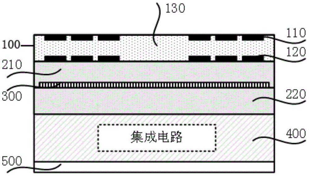
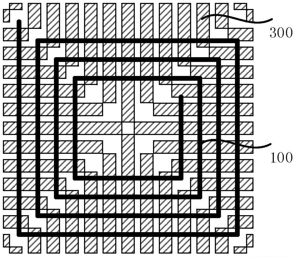
[0017] The invention provides an on-chip integrated transformer, which includes a circuit layer and a transformer layer stacked on the circuit layer, and also includes a shielding layer stacked between the transformer layer and the circuit layer for shielding the electric field formed on the transformer layer. The invention makes the system highly single-chip integrated through the layered design, and can shield the interlayer crosstalk on the transformer layer by adding the shielding layer, so as to ensure the signal and power transmission performance of the transformer layer.

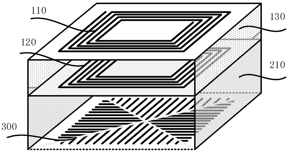
[0018] According to an embodiment of the present invention, the transformer layer may be a transformer on a silicon substrate, including a primary coil, an isolation layer and a secondary coil, the isolation layer is located between the primary coil and the secondary coil, and the primary Coils and secondary coils are formed by helically wound metal wires. The primary coil and the secondary coil trans...


PUM


Abstract

The invention discloses an on-chip integrated transformer, which comprises a circuit layer, a transformer layer and a shielding layer, wherein the transformer layer is stacked on the circuit layer; and the shielding layer is arranged between the transformer layer and the circuit layer and is used for shielding an electric field formed on the transformer layer. Through a stacked design, high chip integration of a system is achieved; through adding the shielding layer, interlayer crosstalk on the transformer layer can be shielded; and the signal and power transmission performance of the transformer layer is ensured.

Description

technical field [0001] The invention belongs to the technical field of integrated circuits, and in particular relates to an on-chip integrated transformer, in particular to an on-chip integrated transformer with a shielding layer in a radio frequency integrated circuit. Background technique [0002] In recent years, with the rapid development of CMOS technology, integration and miniaturization have become the development trend of radio frequency integrated circuits (RFIC). As an important on-chip passive device, silicon-on-chip transformers are widely used in RF integrated circuits to implement functions such as impedance matching, power combining, AC coupling, DC isolation, and bandwidth expansion. [0003] Usually, the transformer on the silicon substrate occupies a relatively large area in the chip. In order to achieve better integration of the circuit and reduce the chip area, the transformer on the silicon substrate and other components in the circuit can be designed in...

Claims


Application Information

Patent Timeline
Patent Type & Authority Applications(China)
IPC IPC(8): H01L27/02H01L23/58H01F27/28H01F27/32
Inventor 张峰屈操
Owner INST OF AUTOMATION CHINESE ACAD OF SCI
Why Eureka
Try Eureka