Capacitive diode assembly and manufacturing method of the capacitive diode assembly

A technology of capacitive diodes and diodes, applied in the field of microelectronics, can solve the problems of high transient power, parasitic effects, poor heat dissipation, and difficulty in achieving TVS devices, and achieve the effects of improving applicability, reducing production costs, and reducing capacitance

Active Publication Date: 2015-12-23
BEIJING YANDONG MICROELECTRONICS
View PDF7 Cites 6 Cited by
  • Summary
  • Abstract
  • Description
  • Claims
  • Application Information

AI Technical Summary

Problems solved by technology

However, due to parasitic effects and poor heat dissipation, it is difficult for this TVS device to achieve high transient power

Method used


Image

  • Capacitive diode assembly and manufacturing method of the capacitive diode assembly
  • Capacitive diode assembly and manufacturing method of the capacitive diode assembly
  • Capacitive diode assembly and manufacturing method of the capacitive diode assembly

Examples


Embodiment Construction

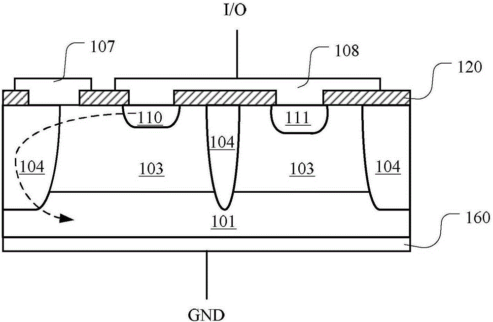
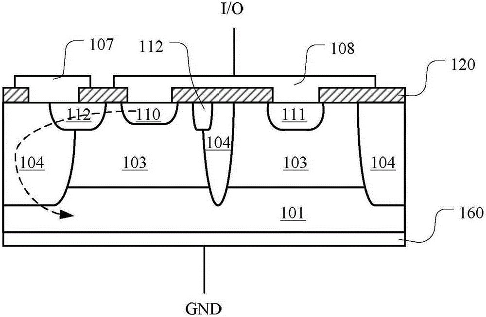
[0035] The present invention will be described in more detail below with reference to the accompanying drawings. In the various figures, like elements are designated by like reference numerals. For the sake of clarity, various parts in the figures have not been drawn to scale. Additionally, some well-known parts may not be shown.

[0036]It will be understood that in describing a structure, when a layer or a region is referred to as being "on" or "over" another layer or region, it can be directly on the other layer or region, or Other layers or regions are also included between it and another layer, another region. And, if the structure is turned over, the layer, one area, will be "below" or "beneath" another layer, another area. In order to describe the situation directly above another layer, another area, the expression "A is directly above B" or "A is above and adjacent to B" will be used herein.

[0037] In addition, a first conductivity type and a second conductivity ...


PUM


Abstract

The invention discloses a capacitive diode assembly and a manufacturing method of the capacitive diode assembly. The capacitive diode assembly comprises a first conductive type of semiconductor substrate, a second conductive type of epitaxial layer which is arranged on the semiconductor substrate, a first conductive type of isolation area, a first conductive type of first doped area, a second conductive type of second doped area and an interconnection structure, wherein the second conductive type is different from the first conductive type; the first conductive type of isolation area; the first conductive type of isolation area penetrates through the epitaxial layer from the surface of the epitaxial layer and extends to the semiconductor substrate so as to restrict a first active area of a first diode and a second active area of a second diode in the epitaxial layer and separate the first active area and the second active area mutually; the first conductive type of first doped area extends to the epitaxial layer from the surface of the epitaxial layer in the first active area; the second conductive type of second doped area extends to the epitaxial layer from the surface of the epitaxial layer in the second active area; and the interconnection structure electrically interconnects a part of the isolation area in the first active area with a part of the epitaxial layer in the first active area. The capacitive diode assembly can be used as a non-polar capacity cell and can improve the transient response speed of a transient voltage inhibitor.

Description

technical field [0001] The present invention relates to the technical field of microelectronics, and more particularly, to a capacitive diode component and a manufacturing method thereof. Background technique [0002] Transient Voltage Suppressor TVS (TransientVoltageSuppressor) is a high-efficiency circuit protection device developed on the basis of voltage regulator tubes. The appearance of TVS diodes is the same as that of ordinary Zener tubes. However, due to the special structure and process design, the transient response speed and surge absorption capacity of TVS diodes are much higher than those of ordinary Zener tubes. For example, the response time of a TVS diode is only 10 -12 seconds and can absorb up to several kilowatts of surge power. In reverse application conditions, when subjected to a large pulse of high energy, the operating impedance of the TVS diode rapidly drops to an extremely low turn-on value, allowing high current flow while clamping the voltage a...

Claims


Application Information

Patent Timeline
Patent Type & Authority Applications(China)
IPC IPC(8): H01L27/08H01L21/822
Inventor 周源张彦秀韦仕贡徐鸿卓
Owner BEIJING YANDONG MICROELECTRONICS
Why Eureka
Try Eureka