Application of P-doped SiC nano wire in field emission cathode material

A field emission cathode and emission cathode technology, applied in the field of nanowire materials, can solve the problems of cutting-edge technology difficulty, preparation difficulty, complex process, etc., and achieve the effects of good cost controllability, stable performance, and uniform diameter

Active Publication Date: 2015-12-30
NINGBO UNIVERSITY OF TECHNOLOGY
View PDF3 Cites 4 Cited by
  • Summary
  • Abstract
  • Description
  • Claims
  • Application Information

AI Technical Summary

Problems solved by technology

However, the cutting-edge technology is difficult, the process is complicated, and the cost is relatively high. For example, carbon nanotubes (open electric field is about 1.79V / μm, field enhancement factor is ~1200); carbon nanocone (open electric field is about 7V / μm) ; Carbon nanorods (open electric field is about 11V / μm), etc., have received extensive attention as cathode emission materials
But at present, the limit opening electric field of the field emission performance of these materials is about 1.5V / μm, and the field enhancement factor is only limited to about 1200, and its preparation is difficult, the process is complicated, and the cost is high.

Method used


Image

  • Application of P-doped SiC nano wire in field emission cathode material
  • Application of P-doped SiC nano wire in field emission cathode material
  • Application of P-doped SiC nano wire in field emission cathode material

Examples


Embodiment 1

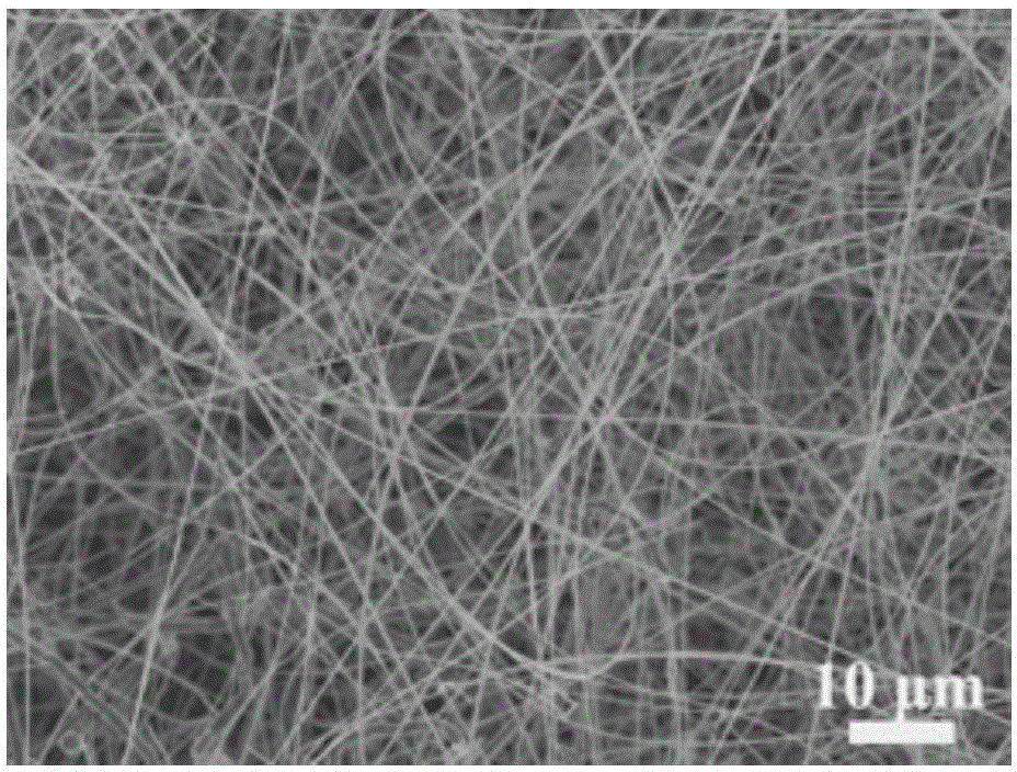
[0055] Select polysilazane, in N 2 Under the protection of the atmosphere, heat-preserve at 260° C. for 30 minutes for thermal cross-linking and curing, put the solidified SiCN solid into a nylon resin ball mill jar, and ball mill and pulverize it into powder.

[0056] Cut carbon paper 5×5cm (length×width), at 0.05mol / LCo(NO 3 ) 3 After soaking in ethanol solution and ultrasonic treatment, take it out and put it in the air environment to dry naturally.

[0057] Weigh 0.3g of polysilazane powder and 0.06g of FePO 4 The powders were mixed and placed at the bottom of a graphite crucible, and the sonicated carbon paper was placed on top of the crucible.

[0058] Put the graphite crucible and carbon paper together in the graphite resistance atmosphere sintering furnace, and the atmosphere furnace is first evacuated to 10 -4 Pa, then fill with high-purity Ar gas (purity is 99.99%), until the pressure is an atmospheric pressure (0.11Mpa), after that the pressure is constant, then...

Embodiment 2

[0060] The only difference from Example 1 is that the pyrolysis temperature is different, and the pyrolysis temperature in Example 2 is 1400°C.

Embodiment 3

[0062] The only difference from Example 1 is that the pyrolysis temperature is different, and the pyrolysis temperature in Example 3 is 1350°C.


PUM

PropertyMeasurementUnit
diameteraaaaaaaaaa
diameteraaaaaaaaaa
aspect ratioaaaaaaaaaa

Abstract

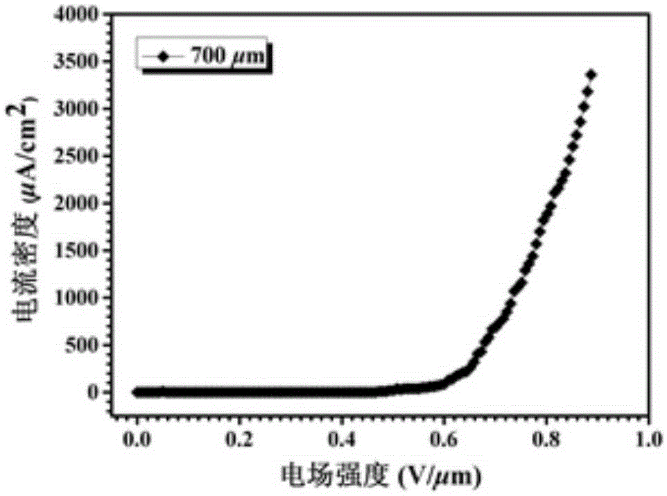
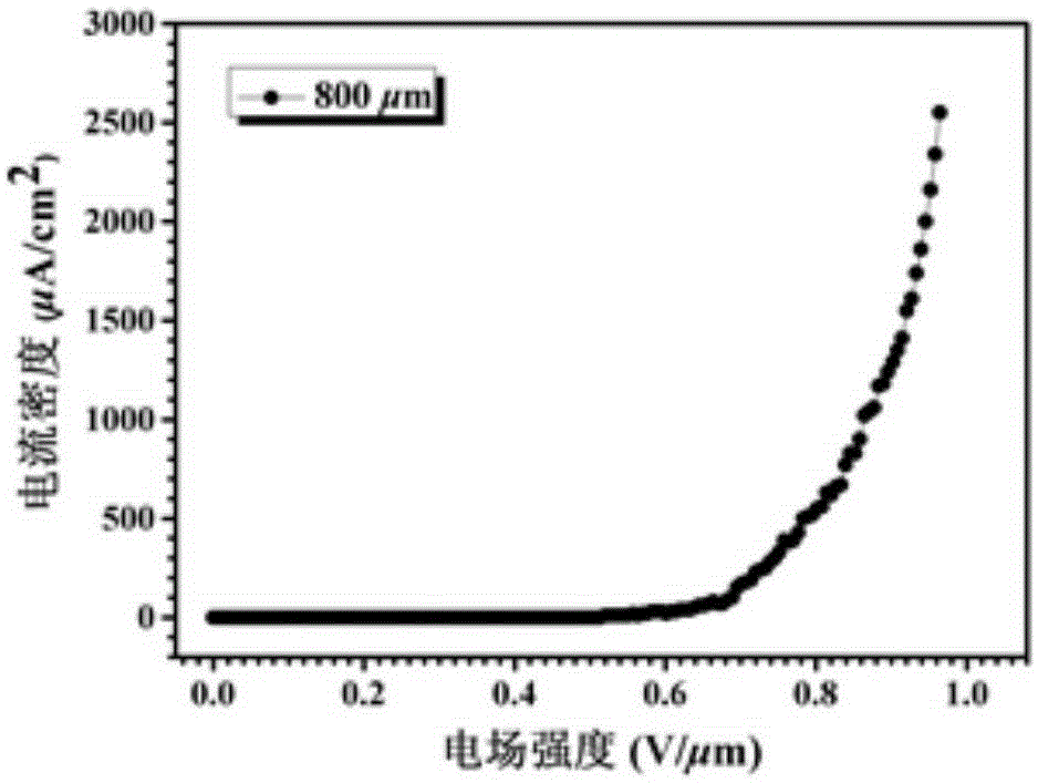
The invention discloses an application of a P-doped SiC nano wire in a field emission cathode material. The P-doped SiC nano wire is a field emission cathode, an emission electric field is formed between the field emission cathode and a field emission anode when voltages are applied, and when the emission current density of the field emission cathode under a normal-temperature vacuum condition is 10 [mu]A/cm<2>, the unlatching field intensity is 0.42 to 0.65 V/[mu]m. The P-doped SiC nano wire provided by the invention has the advantages of low unlatching electric field, good electric field stability and high photoelectric performance.

Description

technical field [0001] The invention relates to a nanowire material used in field emission materials, in particular to the application of P-doped SiC nanowires in field emission cathode materials. Background technique [0002] Field electron emission (field emission) materials have attracted extensive attention and research interest due to their broad application prospects in many high-performance vacuum microelectronic devices such as field emission flat panel displays and electron sources. The two most important quality factors for the performance of field emission materials are current density and turn-on voltage. Because high current density means high brightness, low turn-on voltage means low power consumption. In terms of structure, field emission cathodes can be divided into tip type and thin film type. Initially, the field emission cold cathode structure used a tip-type structure based on the consideration of lowering the threshold voltage, mainly using the charact...

Claims


Application Information

Patent Timeline
Patent Type & Authority Applications(China)
IPC IPC(8): H01J1/304C01B31/36B82Y30/00B82Y40/00
Inventor 杨为佑陈善亮王霖高凤梅杨祚宝
Owner NINGBO UNIVERSITY OF TECHNOLOGY
Why Eureka
Try Eureka