Self-aligned trench power device and manufacturing method thereof

A technology of a power device and a manufacturing method, which is applied in the field of self-aligned trench type power devices, can solve the problems of high cost of photolithography machine, time-consuming device fabrication, unfavorable industrial production, etc., so as to reduce process complexity and trench density. The effect of improving and reducing on-resistance

Active Publication Date: 2019-05-21
FOUNDER MICROELECTRONICS INT
View PDF10 Cites 0 Cited by
  • Summary
  • Abstract
  • Description
  • Claims
  • Application Information

AI Technical Summary

Problems solved by technology

However, due to the reduction in size, the requirements for lithography accuracy are higher. The cost of lithography machines is very expensive, and the depreciation speed is fast when used. The higher the requirements for lithography accuracy, the cost of purchasing lithography machines The higher it is, the longer it will take to make the device, which is not conducive to industrial production

Method used


Image

  • Self-aligned trench power device and manufacturing method thereof
  • Self-aligned trench power device and manufacturing method thereof
  • Self-aligned trench power device and manufacturing method thereof

Examples


Embodiment Construction

[0028] In order to understand the above objects, features and advantages of the present invention more clearly, the present invention will be further described in detail below with reference to the accompanying drawings and specific embodiments. It should be noted that the embodiments of the present application and the features in the embodiments may be combined with each other in the case of no conflict.

[0029] Many specific details are set forth in the following description to facilitate a full understanding of the present invention. However, the present invention can also be implemented in other ways different from those described herein. Therefore, the protection scope of the present invention is not limited by the specific details disclosed below. Example limitations.

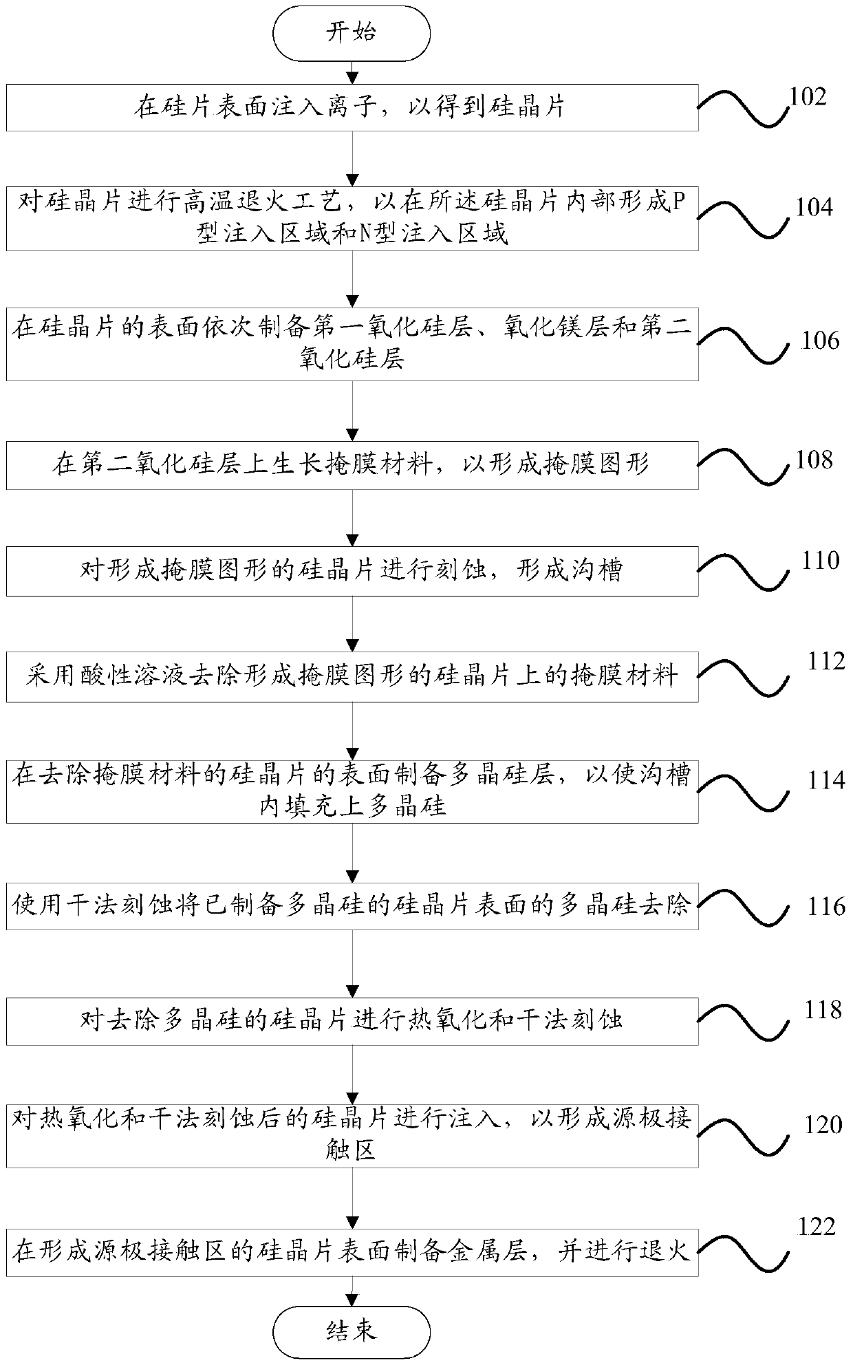
[0030] figure 1 A flow chart of a method for fabricating a self-aligned trench type power device according to an embodiment of the present invention is shown.

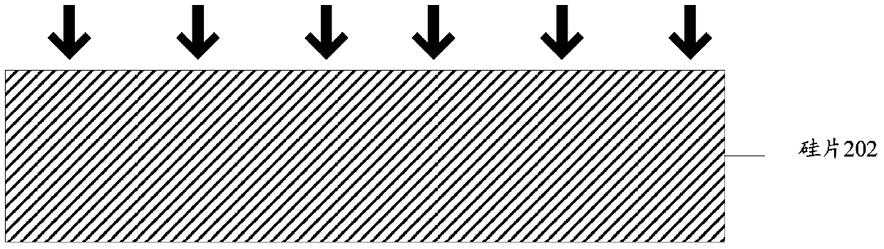
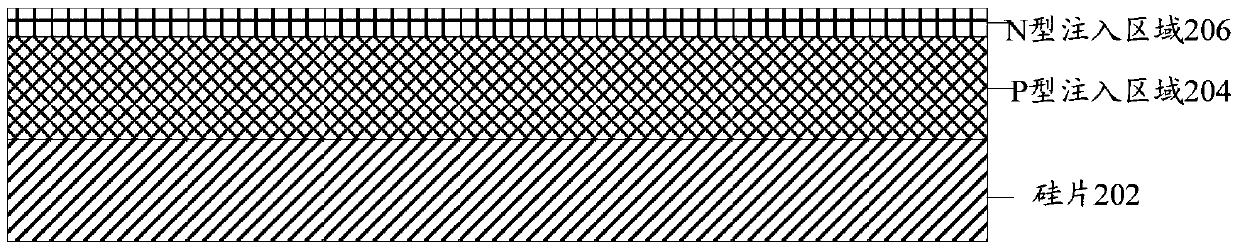
[0031] like figure 1 As shown, the meth...


PUM


Abstract

The invention provides a manufacturing method of a self-aligned trench type power device, which comprises the steps of implanting ions into the surface of a silicon wafer, carrying out high temperature annealing, forming a P-type implantation region and an N-type implantation region, and sequentially preparing a first silicon oxide layer, a magnesium oxide layer and a second silicon oxide layer; growing a mask material on the second silicon oxide layer so as to form a mask pattern; carrying out etching so as to form a trench; removing the mask material by adopting an acid solution; preparing a polycrystalline silicon layer on the surface of the crystal silicon wafer at the moment, and enabling the trench to be filled with polycrystalline silicon; removing the polycrystalline silicon on the surface of the crystal silicon wafer by using dry etching; carrying out thermal oxidation and dry etching; carrying out implantation on the crystal silicon wafer after thermal oxidation and dry etching so as to form a source electrode contact region; and preparing a metal layer on the crystal silicon wafer surface where the source electrode contact region is formed, and carrying out annealing. Correspondingly, the invention further provides a self-aligned trench type power device. Through the technical scheme provided by the invention, the device area is reduced, the on-resistance and the manufacturing cost of the device are reduced, and the device performance is improved.

Description

technical field [0001] The present invention relates to the technical field of semiconductors, and in particular, to a method for manufacturing a self-aligned trench type power device and a self-aligned trench type power device. Background technique [0002] Trench-type power devices are widely used. The drain and source electrodes are located on both sides of the device, allowing the current to flow vertically inside the device, increasing the current density, improving the rated current, and the on-resistance per unit area. [0003] At present, a photolithography process is commonly used to form the source metal contact of the active region of the trench type power device. The photolithography process has high etching accuracy and low defect density. However, in order to integrate more chips in the same area, the size of the adjacent trenches must be reduced. At this time, the more resistors connected in parallel, the smaller the total on-resistance. Therefore, the reducti...

Claims


Application Information

Patent Timeline
Patent Type & Authority Patents(China)
IPC IPC(8): H01L21/762H01L21/336H01L29/06H01L29/78
Inventor 李理马万里赵圣哲
Owner FOUNDER MICROELECTRONICS INT
Why Eureka
Try Eureka